Abstract
The material quality degradation of silicon wafers by metal impurities, various crystal defects as well as light and thermally induced mechanisms is very important for the solar cell performance and has been investigated by various groups. In this paper, the material degradation during epitaxial deposition at high temperatures above 1100°C will be discussed. Annealing experiments in hydrogen atmosphere are done with the laboratory rapid thermal chemical vapor deposition reactor to mimic the thermal process conditions for epitaxial growth of silicon from the gas phase. A general investigation of crystallographic and electronic properties of n- and p-type silicon wafers has been done between 950°C and 1150°C. A detailed sensitivity analysis of process parameters like cooling ramp, peak temperature, duration, and ambient gasses has been conducted. The degradation mechanism by metal impurities has been investigated by using silicon wafers with different diffusion barriers. Besides effective minority carrier lifetime, measurements by quasi steady state photo conductance, etch pit density, Raman spectroscopy, X-ray diffraction, and Fourier transform infrared spectroscopy measurements have been done. The presented results have been used to improve the deposition process of epitaxial thin-film solar cells, the production of silicon foils with a thickness <80 μm, and the fabrication of epitaxial multi junction solar cells with silicon bottom cell.
Introduction
The degradation of silicon material by metal impurities [1, 2], by light and thermally induced degradation [3], and by various crystal defects [4] like grain boundaries, crystal defects, and dislocations including vacancies, stacking faults, and interstitials is a critical factor for the resulting solar cell efficiency.
The described material degradation during the solar cell fabrication can be summarized as Shockley–Read–Hall recombination [5, 6] of excess carriers. Due to improvements in the fabrication processes, the material quality of mc, FZ, and Cz material could be significantly improved by magnetic assisted growth or defect annealing after ion implantation [7, 8].
On the other hand, the degradation of p-type and n-type wafers during the defect annealing [9, 10] and rapid thermal processing [11] in a commercial tube furnace has been reported. Furthermore, during the silicon deposition at temperatures above 1100°C by atmospheric pressure, chemical vapor deposition (APCVD) degradation of the silicon substrate was reported by [12, 13]. Since no conclusive explanation on the origin of this degradation has been presented, a close investigation of the degradation during the epitaxial deposition at high temperatures will be presented in this paper. Degradation is observed after epitaxial growth processes done in the laboratory rapid thermal chemical vapor deposition (RTCVD) reactor in a temperature range of 950°C and 1150°C. To simplify the investigation of degradation, a reference process using the same ambient gas without the trichlorosilane precursor has been used in order to be able to correlate degradation to the thermal process. Based on these experiments, the epitaxial silicon deposition process and the deposition parameters have been adjusted. Subsequently, these findings have been used to fabricate epitaxial p- and n-type emitters which results in an increase in cell efficiency from 18.6% to 23.7% [14].
Methods and Experimental Procedure
The high-temperature annealing processes were carried out in two RTCVD reactors [13, 15, 16]. The laboratory reactors operate at atmospheric pressure and consist of a quartz carrier inside a quartz furnace heated by halogen lamps. Process temperatures between 950°C and 1150°C as well as durations from 4 to 35 min have been varied depending on the experiment. The process times does not include the heating and cooling ramp if not stated otherwise. The heating and cooling ramps between 100 and 150 K min−1 are similar to the APCVD process and remain unchanged. Aside from hydrogen, the ambient gas for the silicon deposition process, argon, and nitrogen were used during the annealing. The reactor tubes as well as the quartz carrier are made of Heraeus HSQ 300 microelectronic-grade material which is also used in commercial diffusion furnaces. The reactor chamber and the carrier were cleaned by HCl etching, and the silicon wafers were chemically polished (CP etching) and cleaned by an RCA sequence prior to the experiment.
Depending on the experiment, n-type and p-type Cz and FZ silicon wafers have been used. The influence of the doping concentration on degradation was investigated by using 1 and 10 Ωcm wafers. In some cases, the wafers were coated with a diffusion barrier prior to the annealing process. In the first experiment, the diffusion barrier is a thermal silicon oxide of 105 or 275 nm thickness grown in a Centrotherm furnace at 950°C.
In a following experiment, an “ONO stack” of SiOx and SiNx by plasma-enhanced chemical vapor deposition (PECVD) was deposited on top of the thermal SiO2 of 105 nm. After the annealing process, the diffusion barrier was etched away, the samples were cleaned by an RCA sequence, and passivated with SiNx or Al2O3 by PECVD or atomic layer deposition (ALD), respectively.
The lifetime measurements have been conducted using a microwave photo conductance decay (MWPCD) setup WT-2000D by Semilab or a quasi steady-state photo conductance (QSSPC) setup by Sinton Instruments. A correction for the carrier diffusion at high lifetimes for MWPCD has been used according to the work of [17]. The QSSPC setup has also been used to determine the iron concentration based on the formation of interstitial iron Fei from iron boron complex FeB under illumination [18, 19]. The evaluation of the crystallographic quality by etch pit density (EPD) has been determined using a white light microscope after surface treatment via Secco etching [20].
Induced defects caused by the annealing process also lead to a lattice mismatch which results in lattice strains. These strains and the responsible defect atoms can be evaluated by μRaman spectroscopy [21] and Fourier transformed infrared spectroscopy (FTIR) [22]. For the FTIR measurements, a Bruker IFS 113 instrument was used to acquire spectra in the range of 400–2500 cm−1 with 6 cm−1 resolution. Additionally, X-ray diffraction (XRD) omega-2theta measurements [23, 24] have been done. The XRD tool used is a Philips X'Pert MRD with a CuKα X-ray (λ = 0.154 nm) source.
Experimental Results and Discussion
Lifetime measurements after high-temperature annealing processes
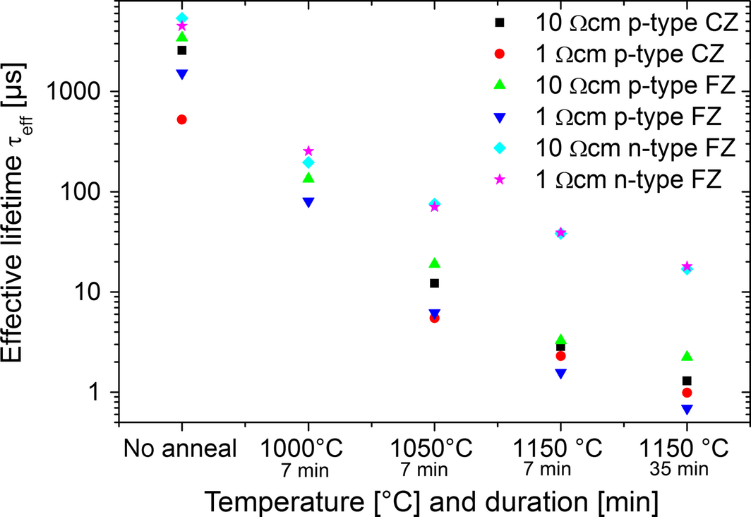
A preliminary experiment was designated to determine the actual material degradation at 1000°C and 1050°C for 7 min as well as at 1150°C for 7 min and 35 min under hydrogen atmosphere. The heating-up and cooling took place with a ramp of 100 K min−1. In Figure 1, the results of the three annealing temperatures for six different silicon wafers including Cz and FZ, n- and p-type as well as 1 and 10 Ωcm are summarized. In this case, all samples have been passivated by SiNx deposited by PECVD and measured by QSSPC. The effective minority carrier lifetime degradation of almost two orders of magnitude to 1.5 μsec for p-type and 39 μsec for n-type FZ wafers with 1 Ωcm after a 7 min annealing process at 1150°C displays the magnitude of the degradation. The change of process time to 35 min shows further degradation in lifetime. A reduction of the annealing temperature to 1000°C lowers the degradation in lifetime to 253 μsec for n-type and 80 μsec for p-type FZ wafers with 1 Ωcm. Aside from the decrease in lifetimes for higher temperatures, it is apparent that the n-type FZ wafers show a slope with lower gradient. This effect can be correlated with a smaller capture cross section of certain defects in n-type silicon [6].
|
|
|
Figure 1. Effective lifetimes for six different silicon wafers processed for 7 min and 35 min, respectively, at three different temperatures. |
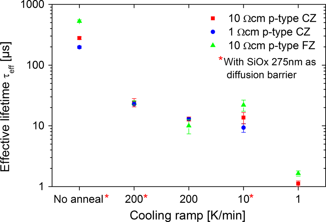
The second experiment examines not only the thermal load of different annealing processes but also the influence of the cooling ramp on the material quality. Each sample was heated up with a ramp of 150 K min−1 from 25°C to 1120°C. After a 4 min anneal at 1120°C, the samples were cooled down with varied cooling ramps from 1120°C to 750°C. The minority-carrier lifetime results are shown in Figure 2. There is an overall decrease of lifetime in the case of 10 Ωcm p-type FZ material from about 500 μsec to below 30 μsec, which is just slightly different for the other materials investigated. Although untreated FZ-material should have lifetime values in the range of ms, in this case, the influence of a low passivation quality is apparent. Since the overall effect of lifetime degradation is still observable, the process-related problems during the passivation will not be discussed.
|
|
|
Figure 2. Lifetime degradation depending on cooling ramp for 200, 10, and 1 K min−1 with and without diffusion barrier processed at RTCVD 100. |
The lifetime degradation by reducing the cooling rate from 200 to 10 K min−1 and 1 K min−1 is related to a change in thermal load and duration of the cooling process. The process time for a cool down from 1120°C to 750°C increases from 2 to 370 min. Furthermore, this experiment investigates the effect of a 275 nm thermal SiO2 diffusion barrier. A few samples had this SiO2 layer, whereas the others had no diffusion barrier at all. Despite an increased lifetime from 13 to 24 μsec (+84%) at 200 K min−1 for samples with diffusion barrier, the significant degradation is not prevented. This result can be explained by the high thermal load and the insufficient quality of thermal SiO2 as diffusion barrier. Additional investigations about SiO2 as diffusion barrier have been done by [25].
Unfortunately, the presented experiments only prove a negative correlation between the thermal budget applied and the minority carrier lifetime, but not if the degradation is caused by the diffusion of impurities or by the generation of crystal defects.
Influence of diffused metal impurities on material degradation
As part of the second experiment, it was shown that 275 nm thermal silicon dioxide did not prevent the lifetime degradation. This leads to the conclusion that SiO2 does not work as a proper diffusion barrier for this experiment under the assumption that metal impurities are responsible for the lifetime degradation. In equation (1), the general definition of the diffusion coefficient Dimpurity of metal impurities [26, 27] depending on the distance between atoms , number of vacant lattice sites N, jump frequency ω, and energy barrier EB is shown.
|
|
(1) |
With the relation between Dimpurity and diffusion time t (annealing time), one obtains the diffusion length L
|
|
(2) |
In Table 1, the diffusivity depending on the temperature and the corresponding diffusion length of three different metal impurities for a 4 min annealing process are listed. In case of iron, the diffusivity changes from 1.6 × 10⁻⁶ m2 sec−1 at 900°C to 5.1 × 10⁻⁶ m2 sec−1 at 1150°C [28, 29]. The corresponding diffusion length for a 4 min annealing process increases from 193 to 349 μm. In case of nickel, the diffusion length at 1150°C is >1000 μm. These values highlight the difference and the critical impact of the diffusion of metal impurities.
| Temperature | DFe [cm² sec−1] | LFe [μm] | DTi [cm² sec−1] | LTi [μm] | DNi [cm² sec−1] | LNi [μm] |
|---|---|---|---|---|---|---|
| 900°C | 1.56 × 10⁻⁶ | 193 | 2.96 × 10⁻¹⁰ | 2.67 | 1.91 × 10⁻⁵ | 678 |
| 1000°C | 2.64 × 10⁻⁶ | 252 | 1.19 × 10⁻⁹ | 5.34 | 2.76 × 10⁻⁵ | 813 |
| 1150°C | 5.08 × 10⁻⁶ | 349 | 6.64 × 10⁻⁹ | 12.6 | 4.33 × 10⁻⁵ | 1020 |
Since a lifetime degradation has been observed for samples with SiO2 as a diffusion barrier, an additional experiment with and without SiO2-ONO-stack as diffusion barrier were annealed in hydrogen for 4 min at 950°C, 1000°C, 1050°C, and 1100°C with a temperature ramp of 150°C min−1. The SiO2-ONO diffusion barrier consists of thermal SiO2 (105 nm) and a layer system of SiOx (1 μm), SiNx (100 nm), and SiOx (1 μm) deposited by PECVD.
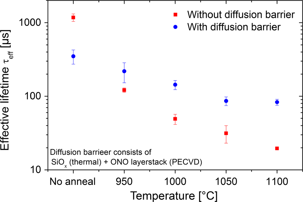
In Figure 3, the lifetime measurements for samples with and without ONO-stack are shown. Again, the figure shows the mean values of three equally processed samples including errors bars. At 1100°C, the lifetime of the 1 Ωcm, p-type FZ sample is reduced to 83 μsec with and to 20 μsec without barrier. The correlation between annealing temperatures and degradation shows a higher gradient for the samples without diffusion barrier. However, despite SiO2-ONO-stack, there is still a significant decline in effective minority carrier lifetime.
|
|
|
Figure 3. Effective lifetime for different annealing temperatures regarding samples with and without ONO-stack as diffusion barrier. |
After annealing, the iron content of the samples was estimated by measurement of FeB complexes in the samples via QSSPC [30] assuming that the metal impurities are the main influence on the lifetime degradation. The samples were measured both after 24 h storage in darkness and after light soaking. The difference in lifetime due to the formation of interstitial iron Fei by dissociation of FeB complexes gives information about the iron content in the sample [31] with a measurement error of about 20 %. The lifetime measurements are injection independent for high FeB concentrations and strongly differ in their shape due to increased SRH-lifetime by Fei after illumination. In Table 2, the iron content of samples with and without SiO2-ONO-stack at four temperatures between 950°C and 1100°C are shown. It is important to note that there is a rise in iron content for samples with and without diffusion layer, even if they were not annealed. The iron content of samples with SiO2-ONO-stack, is increased from below the detection limit (≈ 1.0 × 10⁸ 1 per cm3, without barrier) to approximately 2.1 × 10¹⁰ 1 per cm3. This process-related effect due to the deposition of the SiO2-ONO-stack plays a minor role for annealed samples because the iron concentration in annealed samples of 1011 impurities per cm3 is one order of magnitude higher. The difference in iron concentration depending on the annealing temperature is limited, but in case of the samples without ONO stack, the concentration increases from 1.1 × 10¹¹ 1 per cm3 at 950°C to 4.1 × 10¹¹ 1 per cm3 at 1100°C.
| Type of sample/Temperature | No process | 950°C | 1000°C | 1050°C | 1100°C |
|---|---|---|---|---|---|
| NFe [1 per cm³] with ONO | 2.1 × 10¹⁰ | 1.4 × 10¹¹ | 2.2 × 10¹¹ | 3.3 × 10¹¹ | 2.8 × 10¹¹ |
| NFe [1 per cm³] without ONO | 1.0 × 10⁸ | 1.1 × 10¹¹ | 2.8 × 10¹¹ | 2.7 × 10¹¹ | 4.1 × 10¹¹ |
Corresponding calculations of the Shockley–Read–Hall lifetime depending on the iron concentration have been done to evaluate the measured concentration. The SRH lifetime has been calculated by equation (3) according to [7] using defect energy Et, the carrier concentration in thermal equilibrium n0 and p0 and the capture cross-section and for holes and electrons.
|
|
(3) |
Based on [32] the electron and hole lifetime in thermal equilibrium and the carrier concentration under illumination have been calculated using equation (4) and (5).
|
|
(4) |
|
|
(5) |
The valence band eV and the conduction band eV in crystalline silicon as well as data for different defect centers can be found in [33]. In case of iron impurities,
|
|
(6) |
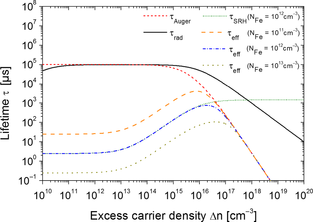
have been used for the calculations. The radiative lifetime τrad and Auger lifetime τAuger have been determined for a 1 Ωcm, p-type, FZ wafer according to [7]. The calculated effective lifetimes τeff are shown in Figure 4. The detrimental effect on the SRH-lifetime τSRH at low injection density is shown for an iron concentration of NFe = 1 × 1012 cm−3. The impact of the metal impurity concentration is depicted by the effective lifetimes for three different iron concentrations. The differences in τeff between NFe = 1 × 1010 cm−3 and NFe = 1 × 1012 cm−3 are approximately two orders of magnitude. These calculations are in agreement with the measured iron concentration and the corresponding lifetime values.
|
|
|
Figure 4. Calculated radiative, auger, and SRH-lifetimes for three different iron concentrations and the resulting effective lifetimes. |
Nevertheless, additional investigations of the degradation effect including different metal impurities are necessary. Therefore, deep level transient spectroscopy (DLTS) [31] and total reflection X-ray fluorescence (TXRF) [27] measurements will be conducted.
However, the degradation by metal impurities alone does not explain the difference between the silicon wafers with and without diffusion barrier. This suggests that there is an additional degradation mechanism. In [9], the impurity diffusion into n-type material during the defect annealing after ion implantation in a diffusion furnace was ruled out due to the fact that the sub-bandgap energy level corresponding to the SRH lifetime did not change.
An explanation of the additional degradation in lifetime is the appearance and propagation of thermal defects induced into the silicon crystal [3]. The reason for a reduced degradation of samples with dielectric layer at higher temperatures could be the reduction of stress and strain on the sample surface [34].
Formation and migration of crystal defects
The formation of crystal defects can be influenced by peak temperature, thermal load, and by the heating and cooling ramp as suggested by [3]. Since the temperature ramps are always associated with the thermal load, a complete separation is very difficult. In theory, a very high temperature gradient is supposed to cause the “freezing” of crystal defects by crossing a specific temperature. The results would be point defects like interstitials or vacancies, dislocations, and stress in the crystalline silicon wafer.
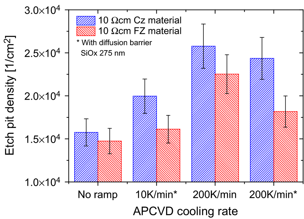
The determination of the crystal defect formation at high temperatures has been evaluated by EPD measurements. In Figure 5, the EPD measurements of the first experiment show a minor increase in defect density of 18–12% by increasing the cooling ramp from 10 to 200 K min−1. The direct comparison of etch pit densities on samples (200 K min−1 cooling ramp) annealed with SiO2 of 1.8 × 10⁴ 1 per cm² and without SiO2 of 2.2 × 10⁴ 1 per cm² in case of FZ material shows the indirect impact of the diffusion barrier. This difference can be explained by the reduced stress on the silicon surface [34] and the positive effect of a diffusion barrier which prevents silicon etching during hydrogen anneal. These results prove that the difference in etch pit density for an annealing process at high temperatures is negligible as one of the main reasons for the material degradation. However, additional experiments are required to have enough statistics for a substantial analysis because the measurement error is about 25–50%. Supplementary EPD measurements of the samples without diffusion barrier show similar etch pit densities after an additional etching of 10 μm by chemical polishing. These measurements demonstrate that there are no additional crystalline defects in the near-surface region. Furthermore, a comparison between the Cz samples without annealing (1.5 × 10⁴ 1 per cm²) and the annealed Cz samples (2.2 × 10⁴ 1 per cm²) show no relevant increase. Since no significant effect in lifetime degradation can be found by various cooling ramps (see Fig. 2), the standard cooling process of 150 K min−1 will remain unchanged.
|
|
|
Figure 5. Etch pit density measurements of samples with and without diffusion barrier after annealing and two different cooling ramps. |
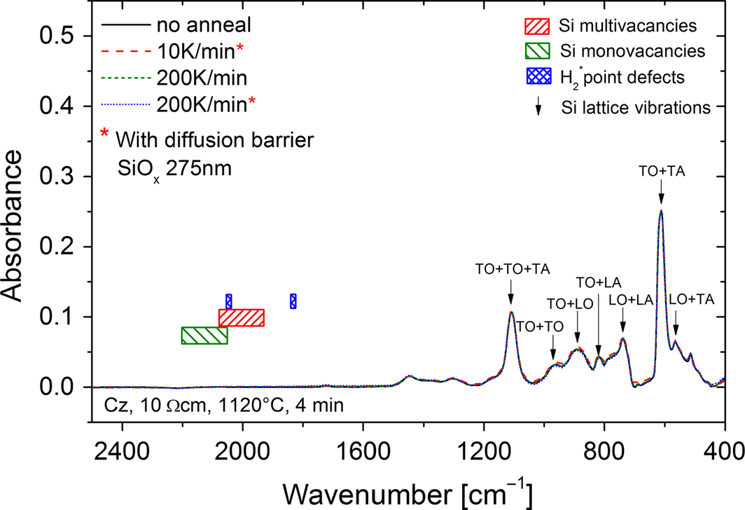
In [35] FTIR spectra have been measured to characterize the crystallographic defects before and after annealing. Based on these experiments, FTIR measurements on FZ and Cz material after annealing using the RTCVD reactor have been done. The measurements in Figure 6 show no additional peak due to crystal defects between 1800 and 2200 nm [35]. Despite the vibrations of the silicon lattice below 1200 nm, no absorbance by vacancies or hydrogen point defects has been detected. Supplementary X-ray diffraction (XRD) omega-2theta measurements [23, 24] of a reference and an annealed wafer at 1100°C have been made. Despite an increase in FWHM from 30.3 to 47.37 arcsec, no significant change in crystal quality is identified. The μRaman measurements have not shown a significant increase in crystal defect density as well because neither an additional defect peak nor an increasing FWHM of the Si peak Lorentz fit could be determined.
|
|
|
Figure 6. Fourier transformed infrared spectroscopy measurements of the silicon wafers after different annealing processes with and without diffusion barrier. The labeled features correspond to transverse acoustic (TA), transverse optic (TO), longitudinal acoustic (LA), and longitudinal optic (LO). |
Process parameters and reactor properties
Since no significant crystallographic degradation has been found, metal impurities seem to be the limiting degradation effect. Therefore, additional experiments have been done to explain the origin of metal impurities The lifetime measurements of 1 Ωcm, p-type, FZ wafers after the different high-temperature oxidation processes (105 nm thermal SiO2 at 950°C, 275 nm at 1050°C) using a diffusion furnace show no significant degradation. Since the same quartz material is used in a commercially available diffusion furnace (validated by INAA measurements at the University of Mainz) and the gasses used have a certified quality of 6N with an additional purification process of the hydrogen by a palladium cell, there is no apparent reason for lifetime degradation in the used RTCVD reactor. The determination of absolute impurity concentration by SIMS or GDMS has been difficult because the concentrations are below the detection limit [30].
The major difference between both annealing processes is the peak temperature of 1150°C during the APCVD process. The duration is similar because the defect annealing, as post processing after the ion implantation, can take up to 60 min. Another difference between a diffusion furnace and the RTCVD reactors is the ambient gasses which are used. At 1120°C, the lifetime of 56 ± 9 μsec for an annealing in Ar atmosphere decreases to values below 10 μsec in hydrogen. The difference in lifetime between Ar and H flow suggest an increased effective diffusion coefficient on the silicon surface in hydrogen atmosphere. This difference in effective diffusion constant results in an increased transport of impurities from the quartz carrier.
Analysis and Conclusions
In summary, it can be stated that the degradation in material quality from τeff > 1 msec to values <10 μsec during an APCVD process is dominated by the diffusion of metal impurities. However, the decrease in lifetime cannot be attributed to metal impurities alone, which suggests an additional crystallographic degradation mechanism. In [3], it is suggested that the dangling silicon bonds at the silicon surface propagate as vacancies into the silicon bulk material at high temperatures. However, if the dangling bonds are saturated by the deposition of a dielectric passivation layer, the thermal degradation by 1 D crystallographic dislocation can be reduced [3]. This hypothesis is supported by various groups reporting on the degradation of p-type and n-type wafers during the defect annealing [9, 10] and rapid thermal processing [11] in a commercial tube furnace. In [2], a discrepancy between DLTS measurements and measured lifetime is shown. Although a different conclusion is drawn, these findings could also suggest an additional degradation mechanism. In case of [9], the impurity diffusion into n-type material during the defect annealing after ion implantation in a diffusion furnace was ruled out as degradation mechanism due to the fact that the sub-band gap energy level corresponding to the SRH lifetime measurements did not change. The results presented in this paper show that the formation of crystal defects is not a dominating factor.
Summary
In this work, an investigation of minority carrier lifetime degradation in silicon wafers during a high-temperature annealing processes in a reactor for epitaxial deposition is presented. The variation of peak temperature and total annealing time shows the significance of these process parameters. Various theories on the formation and influence of thermal defects have been investigated by a thorough electrical and crystallographic characterization. In conclusion, it can be stated that the main effect on lifetime degradation results from metal impurities diffusing into the samples, since a diffusion barrier like an ONO-stack increases the lifetime significantly. In order to obtain the iron content in the samples, specific measurements via QSSPC were done and discovered a positive correlation between the amount of iron atoms in the sample and the annealing temperature in the process. Since comparable annealing experiments in other furnace tubes with the same certified quality of process gasses and quartz material show no degradation in lifetime, the sample placement in the carrier or on a susceptors as well as the ambient gasses have been evaluated. Based on these results, the epitaxial deposition by APCVD in general has been optimized. These findings have been used to optimize the deposition of epitaxial p- and n-type emitters which results in an increase in cell efficiency from 18.6% to 23.7% [14]. Furthermore, these experiments contribute to the fundamental understanding of the different degradation mechanism.
Acknowledgments
The authors express their gratitude to Harald Lautenschlager, Mira Kwaitkowska, Elke Gust, Kai Schillinger, Marion Drießen, Stefan Lindekugel, and Michaela Winterhalder at ISE for their support and input in many valuable discussions. This work has been supported by the BMU in the EpiEm project under contract no. FKZ 0325199A.
Conflict of Interest
None declared.
References
- Schubert, M. C. et al. 2012. Modeling distribution and impact of efficiency limiting metallic impurities in silicon solar cells. Proceedings of the 38th IEEE Photovoltaic Specialists Conference, Austin, Texas, USA, Pp. 286–291.
- Eichhammer, W. et al. 1989. On the origin of rapid thermal process induced recombination centers in silicon. J. Appl. Phys.66:3857–3865.
- Sah, C. T., and C. T. Wang. 1975. Experiments on the origin of process−induced recombination centers in silicon. J. Appl. Phys.46:1767.
- Schwuttke, G. H.1982. Crystal defect problems. Proceedings of the 16th IEEE Photovoltaic Specialists Conference, San Diego, CA, USA, Pp. 327–332.
- Shockley, W., and W. T. J. Read. 1952. Statistics of the recombinations of holes and electrons. Phys. Rev.87:835–842.
- Macdonald, D. H., and L. J. Geerligs. 2004. Recombination activity of iron and other transition metals in p- and n-type crystalline silicon. Proceedings of the 19th European Photovoltaic Solar Energy Conference, Paris, France. P. 492.
- Rein, S.2005. Lifetime spectroscopy – a method of defect characterization in silicon for photovoltaic applications. [Dissertation], Fakultät für Physik, Universität Konstanz, Konstanz.
- Hermle, M. et al. 2011. N-type silicon solar cells with implanted emitter. Proceedings of the 26th European Photovoltaic Solar Energy Conference and Exhibition, Hamburg, Germany, Pp. 875-8,
- Mäckel, H., and K. Varner. 2012. On the determination of the emitter saturation current density from lifetime measurements of silicon devices. Prog. Photovolt.21:850–866.
- Glunz, S. W. et al. 2001. Minority carrier lifetime degradation in boron-doped Czochralski silicon. J. Appl. Phys.90:2397–2404.
- Poggi, A. et al. 1994. Rapid thermal annealing of p-type silicon. J. Electrochem. Soc.141:754.
- Kiefer, F.2009. Untersuchungen zu epitaktischen Emittern an Silizium-Solarzellen und kristallinen Silizium-Dünnschicht-Solarzellen. Diploma, Fakultät für Mathematik und Physik, Albert-Ludwigs-Universität, Freiburg.
- Schmich, E. K.2008. High-temperature CVD processes for crystalline silicon thin-film and wafer solar cells. [Dr. rer. nat. Dissertation], Fachbereich Physik, Universität Konstanz, Konstanz.
- Rachow, T.2014. Deposition and characterisation of crystalline silicon. [Dr. rer. nat. Dissertation], Fachbereich Physik, Universität Konstanz, Konstanz.
- Faller and, F. R., and A. Hurrle. 1999. High-temperature CVD for crystalline-silicon thin-film solar cells. IEEE Trans. Electron Devices46:2048–2054.
- Bau, S.2003. High-temperature CVD silicon films for crystalline silicon thin-film solar cells. [Dissertation], Fakultät für Physik, Universität Konstanz, Freiburg.
- Semilab. 2013. npv-Workshop. Cambery, France.
- Lauer, K. et al. 2008. Effect of iron-boron pairs on crystalline silicon solar cells. Proceedings of the 23rd European Photovoltaic Solar Energy Conference, Valencia, Spain, Pp. 1660–1663.
- Palais, O. et al. 2002. Minority carrier lifetime scan maps applied to iron concentration mapping in silicon wafers. Mater. Sci. Eng., B91–92:216–219.
- Secco d'Aragona, F.. 1972. Dislocation etch for (100) planes in silicon. Solid State Sci. Technol.119:948–951.
- Gundel, P.2011. Neue mikroskopische Opto-Spektroskopie-Messtechniken für die Photovoltaik. [Ph.D], Technische Fakultät Freiburg.
- Boyle, R.. 2008. FT-IR measurement of interstitial oxygen and substitutional carbon in silicon wafers. Thermo Fisher Scientific, Madison, WI.
- Erdtmann, M., and T. A. Langdo. 2006. The crystallographic properties of strained silicon measured by X-ray diffraction. J. Mater. Sci.: Mater. Electron.17:137–147.
- Klug, H. P., and L. E. Alexander, eds. 1974. X-ray diffraction procedures. John Wiley & Sons, New York, NY.
- Reber, S.2000. Electrical confinement for the crystalline silicon thin-film solar cell on foreign substrate. [Ph.D], Fachbereich Physik, Johannes Gutenberg-Universität, Mainz.
- Bentzen, A.2006. Phosphorus diffusion and gettering in silicon solar cells. [Dissertation], Department of Physics, University of Oslo, Oslo.
- Kitagawa, H.2000. Diffusion and electrical propertoies of 3d transition-metal impurities in silicon. Solid State Phenom.71:51–72.
- Weber, E. R.1983. Transition metals in silicon. Appl. Phys. A Solids Surf.A30:1–22.
- Graff, K.1995. Metal impurities in silicon-device fabrication, 1st ed. Springer, Berlin.
- Habenicht, H. et al. 2008. Defect transformation in intentionally contaminated FZ silicon during low temperature annealing. Proceedings of the 23rd European Photovoltaic Solar Energy Conference, Valencia, Spain. Pp. 1933–1937.
- Habenicht, H. et al. 2007. Out-diffusion of metal from grain boundaries in multicrystalline silicon during thermal processing. Proceedings of the 22nd European Photovoltaic Solar Energy Conference Milan, Italy. Pp. 1519–1523.
- Würfel, P., ed. 1995. Physik der solarzellen. Spektrum Akademischer, Heidelberg.
- Istratov, A. A. et al. 1999. Iron and its complexes in silicon. Appl. Phys. A69:13–44.
- Bearda, T. et al. , 2013. Low-temperaure emitter passivation for solar cells bonded to glass. Proceedings of the 28th European Photovoltaic Solar Energy Conference, Paris.
- Moriceau, H. et al. 2012. Smart Cut™: Review on an attractive process for innovative substrate elaboration. Nucl. Instrum. Methods Phys. Res. B277:84–92.
Document information
Published on 01/06/17
Submitted on 01/06/17
Licence: Other
Share this document
claim authorship
Are you one of the authors of this document?
