Abstract
We present 10-nm thick metal alloys created by coevaporation of calcium and silver as transparent top electrode for inverted bulk heterojunction small-molecule organic solar cells (SMOSC). It is shown that such alloys exhibit sufficiently high conductivity to replace previously used thicker (>14 nm) pure Ag contacts. At the same time, Ca:Ag alloys have higher transmittance compared to pure Ag, which is desirable for semitransparent SMOSC where the light passes through the device and the metal contact. We find that a metal contact consisting of 1 nm Ag underlayer and 10 nm Ca:Ag of 1:1 mixing ratio (total Ag content by volume of 6 nm) on glass has an average transmittance in the visible range of 76% with a sheet resistance of 27.1 Ω/□, approaching the performance of ITO while being applied by a much gentler deposition method. Application of 10-nm thick alloys in semitransparent SMOSC lead to transmittance in the visible range Tvis of up to 49% and efficiency η of up to 2.3%, showing superior performance compared to devices with pure Ag top contacts.
Introduction
In recent years, organic solar cells have emerged as a potential cost-efficient alternative to current photovoltaic technologies. New materials and concepts have resulted in certified efficiencies of 12% for a multijunction small-molecule organic solar cell (SMOSC) [1] and 10.7% for polymer organic solar cells [2, 3].
Currently, in research and development of thin-film optoelectronic devices like SMOSC or organic light-emitting diodes, the standard configuration involves a glass substrate coated with a prestructured electrode of a transparent conductive oxide (TCO), for example tin-doped indium oxide (In2O3:Sn, or ITO) or aluminium-doped zinc oxide (AZO) [4]. TCOs are typically deposited by sputtering and provide an excellent combination of transparency and conductivity.
Nonetheless, for devices illuminated or transmitting light through the top contact, TCOs are difficult to apply as sputtering damages the organic material underneath. Despite recent successes with new sputter techniques [5], TCOs are also brittle [6, 7] inhibiting their use in flexible devices. Furthermore, the increase in demand for indium, for example, for flat panel displays, led to strongly fluctuating ITO prices in the last decade.
A possible alternative to TCOs are ultra-thin metal layers [8, 9], which can be thermally evaporated in vacuum and can be applied in the same deposition system as the organic small molecules. Al, Ag, and Au thin films are interesting due to high transmittance in the visible range of the spectrum in case of thin layers. Sufficiently closed layers with suitable morphology, which are required for application in optoelectronic devices, can also exhibit high conductivity. However, evaporation of thin metal films to form stable, interconnected, and smooth surfaces is a challenging task.
Obtaining a suitable morphology depends on a variety of factors, for example, metal type, temperature, evaporation rate [10], solvent treatment [11], substrate [11-13], or surfactants [14-17]. Due to the large number of parameters, different thicknesses for coalescence (the threshold between isolated islands and continuous layers, also referred to as percolation thickness) have been reported with values ranging between 2 nm and more than 15 nm [10, 18-20].
While previous studies demonstrated SMOSC with 4.9% efficiency with transparent metal contacts using 21 nm Ag [21], such thick noble metal layers typically have low light transmittance of less than 40–60% in the visible spectrum [20]. In contrast to that, very thin layers of reactive materials such as calcium may instantaneously oxidize, leading to transparent layers with low conductivity.
Here, we report on combinations of calcium and silver, which are codeposited to achieve intermixed alloys where Ca acts as transparent surfactant and antidiffusion matrix for the highly conductive Ag. We show that high transparency and conductivity can be obtained with such combinations, and that this concept can successfully be transferred to semitransparent SMOSC. For this purpose, we have fabricated two kinds of samples: metal layers on glass to study morphology, optical and electrical properties; and in a second step, SMOSC with the most interesting metal layers as top contact to study the performance of Ca:Ag alloys in devices.
Experimental Methods
The investigated samples are fabricated in a custom-made vacuum system (K.J. Lesker, Tonbridge, UK) at a base pressure of 10−8 mbar, using shadow masks. All samples of each type (either simple metal-only samples on glass, or SMOSC) are made on the same wafer (size 15 × 15 cm²) in one run, ensuring comparable conditions for all layers. During a processing run, intentional variation of specific layers or parameters is possible; in this case, the variation of metal layer thickness and composition.
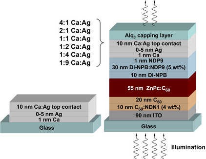
Borofloat 33 glass (Schott, Germany; purchased from Prinz Optics, Stromberg, Germany) cleaned with acetone, ethanol, and oxygen plasma is used as wafer for simple samples that contain only metal layers. The stack consists of 1 nm Ca, 0–5 nm Ag, and 10 nm metal alloys (MA) of different volume mixing ratios (MR), see Figure 1 (left). As MR in the Ca:Ag blend we choose 4:1, 2:1, 1:1, 1:2, 1:4, and 1:9, respectively.
|
|
|
Figure 1. Stack design of metal-only samples (left) and SMOSC (right). The metal-only samples are used to study conductivity and optical properties without influences of organic materials or ITO. |
Such samples are characterized by optical, electrical, and morphological studies. In all cases, the samples are exposed to ambient conditions. Transmittance and reflectance are measured on a Lambda 900 UV/VIS/NIR spectrometer (Perkin Elmer, Waltham, MA) and a UV3100 spectrometer (Shimadzu, Duisburg, Germany). A four-point probe measurement stand S 302-4 (LucasLabs, Gilroy, CA) is used to determine sheet resistances RS of selected samples. The setup is calibrated by characterizing a NIST-traceable indium tin oxide sample (Jandel Engineering Limited, Leighton Buzzard, UK).
Scanning electron micrographs are recorded using a Zeiss DSM 982 Gemini scanning electron microscope (SEM) (Zeiss, Oberkochen, Germany). Several micrographs are recorded at different positions to ensure reproducible results that actually represent the whole sample.
All SMOSC are evaporated onto ITO-coated glass (sheet resistance RS = 32 Ω/□, as measured at IAPP; supplier: TFD, Anaheim, CA) that is cleaned by the same procedure. The devices in the present work are n-i-p type, that is, the intrinsic absorber (i) is embedded between dedicated electron (n) and hole (p) transport materials; the complete stack is shown in Figure 1 (right).
As electron transport layer, 10 nm of C60n-doped by NDN1 (Novaled AG, Dresden, Germany) is used. 20 nm intrinsic C60 serve as extra acceptor for a bulk heterojunction (BHJ) consisting of 1:1 vol. ratio C60 and ZnPc (55 nm thickness), with the substrate being held at 104°C during deposition. For efficient hole transport, 10 nm of intrinsic N,N′-Diphenyl-N,N′-bis(4′-(N,N-bis(naphth-1-yl)-amino)-biphenyl-4-yl)-benzidine (Di-NPB) (Sensient, Bitterfeld-Wolfen, Germany) and an additional 30 nm of Di-NPB doped with 5 wt% NDP9 (Novaled AG [22]) are deposited. For good hole extraction, 1 nm of NDP9 is deposited on the p-Di-NPB. All organic materials except the dopants had been purified at least twice by vacuum gradient sublimation. As surfactant, 1 nm Ca is evaporated as first metal layer on top of the organics. It is expected that this layer reacts with the organic materials, or quickly oxidizes in the processing chamber [23], and acts as transparent antidiffusion layer for the subsequently deposited layers of pure Ag (thickness tAg = (0–5) nm) and 10 nm MA of Ca:Ag. A capping layer of 60 nm tris(8-hydroxy-quinolinato)-aluminum (Alq3) is used as antireflection coating for increased light in/outcoupling [21] into/out of the solar cell.
The completed solar cells are encapsulated with a transparent encapsulation glass, fixed by UV-hardened epoxy glue, in a nitrogen glovebox attached to the vacuum deposition chamber. All samples are stored and subsequently characterized at ambient conditions. The photoactive area of the SMOSC, defined by the overlap between ITO and the metal back contact, is 6.42 mm2 (measured with a light microscope).
Current–voltage J(V) measurements are carried out using simulated AM 1.5G sunlight (16S-150 V.3; Solar Light Co., Glenside, PA). The illumination intensity is kept at (100 ± 1) mW/cm2 monitored by a Si reference diode and is corrected for spectral mismatch. The external quantum efficiency (EQE) is detected using a monochromator and the lock-in technique (Oriel Xe Arc-Lamp Apex Illuminator combined with Cornerstone 260 1/4 m monochromator, both Newport, Irvine, CA; lock-in amplifier 7265 DSP Signal Recovery, Oak Ridge, TN). For EQE, the samples are measured through an aperture of 2.958 mm2.
Results
Optical characteristics of top contacts
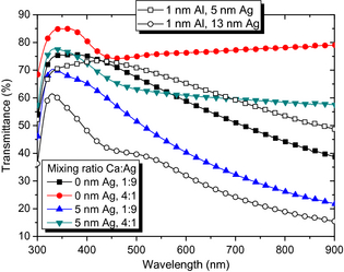
Previous studies have documented that 1 nm Al and 12–16 nm Ag constitute a good combination for SMOSC applications where highly conductive transparent top contacts are needed [24, 25]. However, such films suffer from relatively low light transmittance [24], which is undesirable for this type of application. The data in Figure 2 show that a combination of 1 nm Al and 13 nm Ag on glass (thick reference sample) has a peak transmittance T of just over 60% in the ultraviolet, which then quickly drops to 20–40% in the visible spectrum (380–780 nm) (open circles). While this can be improved with organic light incoupling layers, it would be desirable to have metal combinations with higher intrinsic transmittance.
|
|
|
Figure 2. Filled symbols: transmittance spectra of metal-only samples with a Ca:Ag mixing ratio of 4:1 and 1:9 as well as an Ag interlayer thickness of tAg = 0 nm or 5 nm, on glass. For comparison, the transmittance of two reference electrodes are depicted, using 1 nm Al and 5 nm or 13 nm Ag, respectively (empty symbols). |
Figure 2 also illustrates T of four samples that consist of 1 nm Ca and either 0 nm or 5 nm Ag and an additional 10 nm of Ca:Ag in 1:9 or 4:1 mixing ratio, respectively. The total Ag content ranges from 2 nm (circles), 7 nm (upside-down triangles), 9 nm (squares) up to 14 nm (triangles). All layer combinations exhibit higher T compared to the reference sample, even without capping layers. This is partially understood when considering that Al is not used in these combinations. Furthermore, the highly reactive Ca in the alloys is expected to quickly react with oxygen and water molecules, increasing T [26]. Also, Ca has a low extinction coefficient when compared to other metals such as Al [27] or Ag, such that it is more desirable to include Ca as component or antidiffusion layer in top contacts than other metals.
For comparison, we also show T of a combination of 1 nm Al and 5 nm Ag on glass (thin reference sample) in Figure 2. This metal combination exhibits a series resistance of RS = 27 Ω/□, which is in principle comparable to ITO and should be sufficient for SMOSC application. However, previous studies showed that operational devices could not be obtained with such a thin Ag layer on top of organic materials [28]. The T of 1 nm Al and 5 nm Ag on glass is significantly higher compared to the thick reference sample and is similar to Ca:Ag alloys with high Ca content. This leads to the question if the alloys can successfully be implemented as top contacts with high T, in contrast to 1 nm Al and 5 nm Ag which turned out to have unfavorable morphology and no interpenetrating network on top of a complete SMOSC (see Fig. S1 in the supplementary material).
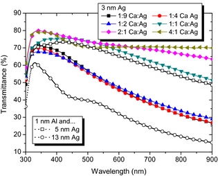
We study additional samples where the Ag interlayer thickness is kept constant at tAg = 3 nm Ag, and the Ca:Ag mixing ratio is varied from 4:1, 2:1, 1:1, 1:2, 1:4 to 1:9, as seen in Figure 3. The data underline that even with 3-nm Ag underlayer, any Ca:Ag alloy exhibits higher average transmittance than the thick reference contact. Generally, high Ca contents lead to high T; however, the exact detailed wavelength-dependent T behaviour is expected to be influenced by various factors, for example, thin film optical effects or the morphology of the coevaporated alloy.
|
|
|
Figure 3. Transmittance of metal-only samples on glass with tAg = 3 nm and different mixing ratios of 10 nm thick layers of Ca:Ag. Shown for comparison are the transmittances of a thin reference contact (1 nm Al, 5 nm Ag) and a thick reference contact (1 nm Al, 13 nm Ag) on glass. |
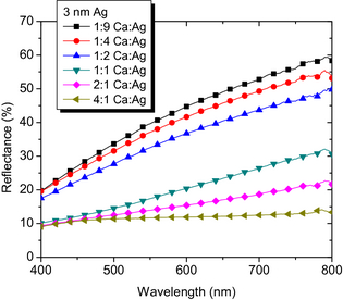
The reflectance R of such samples is shown in Figure 4. Generally, the lower the Ag content (and the higher the Ca content), the lower is the reflection. Especially for MR 2:1 and 4:1, R < 20% in the visible spectrum, which is a vast improvement compared to high R of up to 50% to 60% for the samples with high Ag content in the alloy layer. It is striking that the wavelength dependence is strongly reduced with increasing Ca content. However, this is in accordance with previous studies which found variations of only 20% of the refractive index of Ca [27], compared to, for example, variations of over 150% for aluminum [27] or silver [29].
|
|
|
Figure 4. Reflectance of samples on glass with tAg = 3 nm and different mixing ratios of 10 nm thick Ca:Ag blends. |
In summary, all alloys have superior optical properties compared to the thick reference and are hence extremely interesting for solar cell applications. To further evaluate their suitability, electrical characterizations are desirable.
Electrical characteristics of top contacts
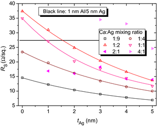
Sheet resistances RS of combinations of 1 nm Al and 2–15 nm Ag on glass were shown in the literature [24]; a contact of 1 nm Al and 5 nm Ag exhibited RS = 27 Ω/□ (shown as horizontal black line in Fig. 5), which is in the range of the ITO used in the current work (32 Ω/□, as measured in the same way like the metal layers). For pure Ag electrodes with thicknesses above 10 nm, RS < 5 Ω/□ is routinely achieved; however, this leads to strong decreases in T.
|
|
|
Figure 5. Sheet resistances RS of various samples of metal blend layers on glass, having tAg = 0–5 nm and different mixing ratios (MR) of Ca:Ag. The horizontal black line marks the RS = 27 Ω/□ that is obtained from 1 nm Al/5 nm Ag on glass [24], which, however, did not work in SMOSC applications. Lines: fits of the 1:9, 1:4, 1:2, and 1:1 MR; the fit is a guide to the eye. Full symbols: 2:1 and 4:1 MR. |
The data in Figure 5 represent samples with 1 nm Ca and different metal combinations. They demonstrate that almost all alloys exhibit better sheet resistances than our ITO (32 Ω/□), and values below 20 Ω/□ are easily achieved. The fit is a guide to the eye; as the empirical fit shows, the presence of Ag underlayers leads to a decrease of RS with increasing Ag thickness for 1:9, 1:4, 1:2, and 1:1 Ca:Ag MR.
The resistive properties of thin films have been studied in the literature. Based on electron scattering from surfaces and grain boundaries, the Mayadas–Shatzkes [30] (MS) model has been used as basis to fit experimental measurements, and numerous groups have modified or amended the model to fulfill their requirements. For our experimental data, we chose not to attempt any numerical modeling, as our films contain a mixture of different elements (Ag, Ca, and organic molecules [31]) and compounds; we currently cannot characterize the films in sufficient spatial resolution and chemical composition such that a meaningful explanation of a numerical fit would be within the scope of this study.
The average transmittances Tvis in the visible range from (380–780) nm and the measured sheet resistances for samples of special interest are summarized in Table 1. We have chosen samples that cover a wide range of parameters (variation of tAg and mixing ratio) and are studied in solar cell devices, as described later in Section III. D. For comparison, the thick reference contact shown in Figure 3 (with 1 nm Al, 13 nm Ag) has Tvis = 34% with 4.9 Ω/□; the thin reference (1 nm Al, 5 nm Ag) has a higher Tvis = 67% with 27.4 Ω/□, but could not successfully be integrated into SMOSC.
| tAg | MR | RS | Tvis | tAg | MR | RS | Tvis | |
|---|---|---|---|---|---|---|---|---|
| ||||||||
| 0 | 1:1 | 34.9 | 76 | 3 | 4:1 | 34.5 | 71 | |
| 1 | 1:1 | 27.1 | 76 | 3 | 2:1 | 18.3 | 72 | |
| 2 | 1:1 | 20.2 | 73 | 3 | 1:1 | 17.7 | 69 | |
| 3 | 1:1 | 17.7 | 69 | 3 | 1:2 | 20.4 | 50 | |
| 4 | 1:1 | 14.4 | 63 | 3 | 1:4 | 13.5 | 49 | |
| 5 | 1:1 | 11.7 | 57 | 3 | 1:9 | 8.9 | 50 | |
It is visible that the alloys have higher sheet resistances than the thick reference; however, many compositions achieve even higher Tvis and lower RS than the thin reference, and all samples exhibit Tvis ≫ 34%. The ITO, for comparison, has Tvis = 84% [24] and 32 Ω/□. This is still superior compared to the alloys; however, the combination of 1-nm Ag underlayer with MR 1:1 (Tvis = 76%; RS = 27.1 Ω/□) comes close to this benchmark and has the advantage that it can be processed even by evaporation onto organic materials.
It is expected that T could further be improved by using suitable capping layers to come even closer to the performance of ITO, or to tailor the T to complement specific properties of any SMOSC. This optimization would, however, have to be performed for each combination of organic absorber materials or for each wavelength range and is not expected to contribute significantly to the current manuscript.
Interestingly, the sheet resistance of the 1:1 sample is lower compared to the 1:2 blend, which is against expectation. It seems that the presence of Ca in the right concentration has a positive influence on the film conductivity, possibly induced by morphology changes, phase changes (such that Ca or Ag change from an amorphous to a polycrystalline phase) or formation of a highly conductive blend phase (also indicated by the large step in Tvis).
Morphology of top contacts
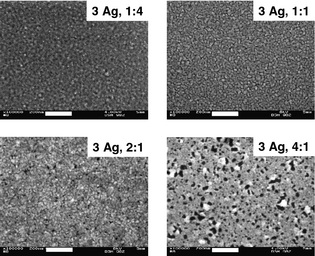
Figure 6 displays scanning electron micrographs of metal-only samples with 3 nm Ag underlayer and different 10-nm thick alloys (1:4, 1:1, 2:1, and 4:1 MR of Ca:Ag) on glass. The images show qualitatively that the morphology changes considerably, depending on the MR. At 1:4 MR (total Ag content of 11 nm), a relatively uniform featureless surface is observed. At 1:1 MR (total Ag content 8 nm), a network with considerable cracks has formed. However, the layer seems to be well-interconnected with sufficient percolation pathways.
|
|
|
Figure 6. SEM micrographs of alloys with different MR of Ca:Ag on 3-nm Ag underlayer. The white scale bars represent 200 nm. |
Black spots in the image at 2:1 MR (6.3 nm Ag) indicate round well-pronounced cracks and defects. Such phenomena are even more distinguished in the 4:1 MR (5 nm Ag) sample. Even though the acceleration voltage is reduced from 8 kV (1:1 and 2:1 MR) to only 4 kV for this sample, considerable amounts of bright grains are visible. These areas suffer from strong charging effects and are likely to have insufficient conductivity. We speculate that these grains may be Ca clusters with weak connection to the percolation network, or which are partially oxidized and hence have reduced conductivity. Additionally, the surface coverage with black spots is increased, which could also explain the increased sheet resistance.
Organic solar cells
We briefly compare the influence of changing the Ag underlayer thickness tAg from 0 nm to 4 nm for a fixed mixing ratio (1:1), and in more detail the influence of the mixing ratio for a fixed tAg = 3 nm.
The device fingerprints for SMOSC with MR = 1:1 and tAg = 0–4 nm are shown in Table 2. The open circuit voltage VOC is similar for all devices and with 0.51 V typical for ZnPc:C60 BHJs, indicating that the changes of top contact composition have no influence on this parameter. As we observe no S-kink in the J(V) curves, we expect good electrical contact of organic materials and top electrode in all devices. A small but systematic variation is visible for the fill factor (FF), which increases from 46% to 51% with increasing tAg. The FF is usually attributed to be influenced by recombination mechanisms, in this case influenced by the electrode. Better RS, as obtained for higher tAg, fits to increasing FF and leads to the conclusion that a certain metal thickness is necessary to achieve suitable top contact morphology for efficient charge carrier extraction.
| tAg (nm) | JSC (mA/cm2) | VOC (V) | FF (%) | η (%) | Tvis (%) |
|---|---|---|---|---|---|
| 0 | 7.0 ± 0.1 | 0.51 | 46 | 1.6 ± 0.1 | 49 |
| 1 | 7.6 ± 0.1 | 0.51 | 49 | 1.9 ± 0.1 | 46 |
| 2 | 7.8 ± 0.1 | 0.51 | 49 | 1.9 ± 0.1 | 44 |
| 3 | 7.9 ± 0.1 | 0.51 | 50 | 2.0 ± 0.1 | 41 |
| 4 | 7.9 ± 0.1 | 0.51 | 51 | 2.0 ± 0.1 | 38 |
The lowest JSC = (7.0 ± 0.1) mA/cm2 for tAg = 0 nm corresponds to the lowest FF and confirms a charge carrier loss due to inferior extraction at the top contact that disappears with higher tAg; for thicknesses between 1–4 nm, only minimal changes are observed, indicating that a 10-nm thick 1:1 alloy easily forms a closed film with suitable conductivity even on organic layers.
From literature, we know semitransparent ZnPc:C60-based SMOSC with optimized 1-nm Al/14 nm Ag top contacts that exhibit 36% transmittance in the visible range with additional light incoupling layers [32] and an efficiency of 2.1%. Our current measurements show that this can be surpassed with Ca:Ag alloys, showing the potential of this concept.
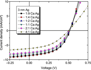
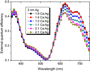
While the influence of tAg on device properties is as anticipated, the question remains to what extent the composition of the alloy may influence SMOSC performance. The device fingerprints for SMOSC with fixed tAg = 3 nm (corresponding to the SEM images) and varying MR are shown in Table 3, with the characteristic J(V) curves under illumination displayed in Figure 7 and the EQE in Figure 8.
| MR Ca:Ag | JSC (mA/cm2) | VOC (V) | FF (%) | η (%) | Tvis (%) |
|---|---|---|---|---|---|
| 4:1 | 6.3 ± 0.1 | 0.5 | 43 | 1.4 ± 0.1 | 44 |
| 2:1 | 7.6 ± 0.1 | 0.51 | 49 | 1.9 ± 0.1 | 46 |
| 1:1 | 7.9 ± 0.1 | 0.51 | 50 | 2.0 ± 0.1 | 41 |
| 1:2 | 8.4 ± 0.1 | 0.51 | 51 | 2.2 ± 0.1 | 38 |
| 1:4 | 8.6 ± 0.1 | 0.52 | 51 | 2.3 ± 0.1 | 38 |
| 1:9 | 8.4 ± 0.1 | 0.52 | 50 | 2.2 ± 0.1 | 39 |
|
|
|
Figure 7. Current voltage data of SMOSC with tAg = 3 nm and different mixing ratios. The devices are illuminated through the bottom, that is, the ITO-coated substrate. |
|
|
|
Figure 8. External quantum efficiency of SMOSC with tAg = 3 nm and different mixing ratios. |
The measurements show that VOC is again almost independent of the metal alloy composition. The slight increase from 0.50 to 0.52 V can be partially explained by an increased quasi-Fermi level splitting in the photoactive layers. With increasing silver content the reflectivity of the back electrode increases, photon and charge carrier densities in the BHJ are enhanced, and the Fermi levels shift towards the corresponding transport levels. Thus, also JSC is improved from 6.3 to 8.6 mA/cm2.
For the SMOSC with the lowest total Ag content (MR 4:1, i.e., a total nominal Ag thickness of 5 nm), we observe the lowest FF = 43% and JSC = (6.3 ± 0.1) mA/cm2. The slope of J(V) in Figure 7 in forward direction suggests that MR 4:1 also leads to the highest series resistance, supporting that a suboptimal metal contact is likely to be responsible for the rather bad device performance. This is attributed to a not fully formed percolation network with isolated Ag clusters embedded in a Ca matrix with low conductivity. The power conversion efficiency is hence limited to η = 1.4% due to similar, although more pronounced effects comparable to our observations for the sample with 0 nm Ag and MR 1:1 as discussed above.
However, with 2:1 MR (total nominal tAg = 6.3 nm), η increases by 50% to (1.9 ± 0.1)% due to higher FF = 49% and JSC = 7.6 mA/cm2. We attribute the higher FF to lower series resistance and better charge carrier collection at the metal electrode, and the higher JSC to higher reflection at the metal contact (leading to a more intense second pass through the absorber) combined with lower recombination.
The FF saturates at (50 ± 1)% and is similar for nominal total Ag contents of (6.3–12) nm, indicating that a sufficiently good metal network is formed for efficient charge carrier extraction for any MR from 2:1 to 1:9. Variations of JSC, which ranges from (7.6–8.6) mA/cm2, are hence attributed to differences in reflectance of the metal contact, as seen in Figure 4.
The EQE data, shown in Figure 8, support that the increase in photocurrent is due to optical effects and correlated to the reflectivity of the metal electrode: the reflectance of Ag is much higher compared to (possibly oxidized) Ca, as seen in Figure 4. The higher reflectance of higher Ag contents allows more photons a second pass through the device, that is, the absorber layers. This increases the chance of absorption and hence the photocurrent.
Strong changes are visible in the ZnPc absorption range from 600–700 nm, with absolute increases of up to 10% when comparing 4:1 and 1:9 MR at 670 nm. Here, also the changes in reflectivity are strong. In contrast to that, EQE in the absorption range of C60, for example, at 450 nm, is almost unaffected with changes <2%. If the SMOSC were decisively influenced by electrical effects, we would have expected uniform changes in the whole spectrum. However, the improvement is clearly wavelength-dependent and correlates to the optical field distribution in the device, which is increased in the absorption range of ZnPc at the BHJ position.
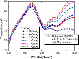
The transmittance in the visible range for tAg = 3 nm and different MR is illustrated in Figure 9, as measured through the ITO bottom contact. As expected, the SMOSC with the smallest nominal tAg in the top electrode exhibit the highest T, with Tvis = 44% for MR 4:1. Shown for comparison is the transmittance of an optimized device known from literature with 1-nm Al/14 nm Ag and an organic capping layer which achieved η = 2.1% (empty diamonds) [32]. It is visible that even the SMOSC of the current work with the highest tAg have higher T than this optimized device, in addition to higher η = (2.2–2.3)% for MR 1:9 and 1:4, respectively. It is likely that a tailored Alq3 capping layer or a suitable distributed Bragg reflector could be used to even further enhance T by optimizing the optical field distribution for MR 2:1 or 1:1 samples, which have sufficiently good electrical properties. Such optimization has been performed for metal contacts in the past [21, 33], but is omitted here as it is not expected to contribute significantly to our understanding of the metal alloy layers.
|
|
|
Figure 9. Filled symbols: transmittance of SMOSC with tAg = 3 nm and different mixing ratios. Empty symbols: reference sample with a pure 14-nm Ag layer as top contact, as measured through the substrate side. |
Conclusion
We have shown that alloys of the noble metal Ag and a reactive metal like Ca are suitable as transparent top contact for organic solar cells. With such combinations, it is possible to fabricate SMOSC with a lower Ag content in the electrode; operational devices are obtained with nominal Ag thicknesses of 5 nm. This is a vast improvement compared to previous work, where 12–14 nm Ag were necessary for an efficient electrical contact. In addition to lower costs, the incorporation of Ca also leads to top contacts with higher transmittance compared to pure thick Ag layers, which is desirable for top-illuminated or semitransparent devices.
Acknowledgments
This work has been supported by the Bundesministerium für Bildung und Forschung in the framework of the InnoProfile Transfer (03IPT602A) project. We thank Ellen Kern from TU Dresden for the SEM measurements.
Conflict of Interest
None declared.
References
- Heliatek Consolidates its Technology Leadership. Press release. Available at http://www.heliatek.com/wp-content/uploads/2013/01/130116_PR_Heliatek_achieves_record_cell_effiency_for_OPV.pdf (accessed 18 December 2013).
- You, J., L. Dou, K. Yoshimura, T. Kato, K. Ohya, T. Moriarty, et al. 2013. A polymer tandem solar cell with 10.6% power conversion efficiency. Nat. Commun.4:1446.
- Green, M. A., K. Emery, Y. Hishikawa, W. Warta, and E. D. Dunlop. 2014. Solar cell efficiency tables (version 43). Prog. Photovoltaics Res. Appl.22:1–9.
- Schulze, K., C. Uhrich, R. Schueppel, K. Leo, M. Pfeiffer, E. Brier, et al. 2007. Organic solar cells on indium tin oxide and aluminium doped zinc oxide anodes. Appl. Phys. Lett.91:073521–073523.
- Lunt, R. R., and V. Bulovic. 2011. Transparent, near-infrared organic photovoltaic solar cells for window and energy-scavenging applications. Appl. Phys. Lett.98:113305.
- Chen, Z., B. Cotterell, W. Wang, E. Guenther, and S. J. Chua. 2001. A mechanical assessment of flexible optoelectronic devices. Thin Solid Films394:202–206.
- Sierros, K. A., N. J. Morris, K. Ramji, and D. R. Cairns. 2009. Stress-corrosion cracking of indium tin oxide coated polyethylene terephthalate for flexible optoelectronic devices. Thin Solid Films517:25902595.
- Oyamada, T., S. Sugawara, Y. Terao, H. Sasabe, and C. Adachi. 2007. Top light-harvesting organic solar cell using ultrathin Ag/MgAg layer as anode. Jpn. J. Appl. Phys.46:1734.
- Pode, R. B., C. J. Lee, D. G. Moon, and J. I. Han. 2004. Transparent conducting metal electrode for top emission organic light-emitting devices: Ca-Ag double layer. Appl. Phys. Lett.84:4614–4616.
- Sennett, R. S., and G. D. Scott. 1950. The structure of evaporated metal films and their optical properties. J. Opt. Soc. Am.40:203–211.
- Roark, S. E., and K. L. Rowlen. 1994. Thin Ag films - influence of substrate and postdeposition treatment on morphology and optical properties. Anal. Chem.66:261–270.
- Duerr, A. E., F. Schreiber, M. Kelsch, H. D. Carstanjen, and H. Dosch. 2002. Morphology and thermal stability of metal contacts on crystalline organic thin films. Adv. Mater.14:961.
- Zaporojtchenko, V., K. Behnke, A. Thran, T. Strunskus, and F. Faupel. 1999. Condensation coefficients and initial stages of growth for noble metals deposited onto chemically different polymer surfaces. Appl. Surf. Sci.144145:355359.
- Camarero, J., J. Ferron, V. Cros, L. Gomez, A. L. de Vazquez, J. M. Gallego, et al. 1998. Atomistic mechanism of surfactant-assisted epitaxial growth. Phys. Rev. Lett.81:850.
- Rosenfeld, G., R. Servaty, C. Teichert, B. Poelsema, and G. Comsa. 1993. Layer-by-layer growth of Ag on Ag(111) induced by enhanced nucleation: a model study for surfactant-mediated growth. Phys. Rev. Lett.71:895–898.
- LeGoues, F. K., B. D. Silverman, and P. S. Ho. 1988. The microstructure of metalpolyimide interfaces. J. Vac. Sci. Technol., A6:2200–2204.
- Thran, A., T. Strunskus, V. Zaporojtchenko, and F. Faupel. 2002. Evidence of noble metal diffusion in polymers at room temperature and its retardation by a chromium barrier. Appl. Phys. Lett.81:244–246.
- Brandt, T., M. Hoevel, B. Gompf, and M. Dressel. 2008. Temperature- and frequency-dependent optical properties of ultrathin Au films. Phys. Rev. B78:205409.
- Granqvist, C. G.2007. Transparent conductors as solar energy materials: a panoramic review, Solar Energy Mater. Solar Cells91:1529–1598.
- Meiss, J., N. Allinger, C. Falkenberg, K. Leo, and M. K. Riede. 2009. Transparent conductive layers for organic solar cells: simulation and experiment. Proc. SPIE7416:741603.
- Meiss, J., T. Menke, K. Leo, C. Uhrich, W. M. Gnehr, S. Sonntag, et al. 2011. Highly efficient semitransparent tandem organic solar cells with complementary absorber materials. Appl. Phys. Lett.99:043301.
- Meyer, J., S. Hamwi, S. Schmale, T. Winkler, H. H. Johannes, T. Riedl, et al. 2009. A strategy towards p-type doping of organic materials with HOMO levels beyond 6 eV using tungsten oxide. J. Mater. Chem.19:702.
- Scholz, S., Q. Huang, M. Thomschke, S. Olthof, P. Sebastian, K. Walzer, et al. 2008. Self-doping and partial oxidation of metal-on-organic interfaces for organic semiconductor devices studied by chemical analysis techniques. J. Appl. Phys.104:104502-1–104502-10.
- Meiss, J.2011. New material concepts for organic solar cells. Optimus Verlag, Göttingen.
- Meiss, J., M. Riede, and K. Leo. 2009. Optimizing the morphology of metal multilayer films for indium tin oxide (ITO)-free inverted organic solar cells. J. Appl. Phys.105:063108.
- Lee, S. N., S. W. Hwang, and C. H. Chen. 2007. Thin-film encapsulation of thin-cathode organic light-emitting devices. Jpn. J. Appl. Phys.46:7432–7435.
- Ramsdale, C. M., and N. C. Greenham. 2003. The optical constants of emitter and electrode materials in polymer light-emitting diodes. J. Phys. D: Appl. Phys.36:L29–L34.
- Meiss, J., M. K. Riede, and K. Leo. 2009. Towards efficient tin-doped indium oxide ITO-free inverted organic solar cells using metal cathodes. Appl. Phys. Lett.94:013303-1–013303-3.
- Palik, D. E. 1985. p. 759. Handbook of optical constants of solids. Vol. 1, Academic Press handbook series Academic Press, Orlando.
- Mayadas, A. F., M. Shatzkes, and J. F. Janak. 1969. Electrical resistivity model for polycrystalline films: the case of specular reflection at external surfaces. Appl. Phys. Lett.14:345.
- Olthof, S., J. Meiss, B. Luessem, M. K. Riede, K. Leo. 2011. Photoelectron spectroscopy investigation of thin metal films employed as top contacts in transparent organic solar cells. Thin Solid Films519:1872–1875.
- Meiss, J., K. Leo, M. K. Riede, C. Uhrich, W. M. Gnehr, S. Sonntag, et al. 2009. Efficient semitransparent small-molecule organic solar cells. Appl. Phys. Lett.95:213306-1–213306-3.
- Meiss, J., M. Furno, S. Pfuetzner, K. Leo, and M. Riede. 2010. Selective absorption enhancement in organic solar cells using light incoupling layers. J. Appl. Phys.107:053117-1–053117-7.
Document information
Published on 01/06/17
Submitted on 01/06/17
Licence: Other
Share this document
Keywords
claim authorship
Are you one of the authors of this document?
