Abstract
This article presents a design, output voltage and inductor current regulations of the negative output elementary boost converter (NOEBC) operated in continuous conduction mode (CCM) using sliding mode controller (SMC) plus proportional double integral controller (PDIC). The NOEBC is a dc–dc converter that can provide high voltage transfer gain, high efficiency, and reduced output voltage and inductor current ripples in comparison with the conventional boost converter. Owing to the time varying switched mode operation, the dynamic characteristics of the NOEBC is non-linear and the designed SMC plus PDIC aims at enhancing the dynamic characteristics along with the inductor current and the output voltage regulations of the NOEBC. The proposed SMC is more appropriate to the essentially variable-structured NOEBC when represented in the state-space average based model. Here, the PDIC suppresses the steady state error and excellent initial start-up response of NOEBC in spite of input supply voltage and load resistance variations. The performance of the SMC plus PDIC is verified for its robustness to perform over a broad range of working conditions in MATLAB/Simulink models as well as in the experimental with the comparative study of a SMC plus proportional-integral-controller (PIC). Simulation and experimental results are presented.
Keywords
DC–DC power conversion; Negative output elementary boost converter; Sliding mode controller; Proportional double-integral controller; State-space average model
1. Introduction
In modern days, the dc–dc conversion topologies are developing very fast and it is more suitable for various medical equipment, power supply for telecommunication network, power supply for computer hardware parts, robot systems, defense electronic power supplies, renewable energy power systems, military applications and many more [1], [2] and [3]. In theoretical point of investigations, the conventional dc–dc converters such as the buck, boost, buck–boost, Cuk, SEPIC (single-ended primary inductor converter), and Zeta converter can achieve a huge voltage transfer gain through an extremely high duty cycle [4], [5], [6], [7] and [8]. However wretchedly, in real-time practice, which is limited due to the effect of power semiconductor switches, rectifier power diodes and the equivalent series resistance (ESR) of storage elements. Furthermore, the extremely huge duty-cycle operation of the converter will affect in a grave reverse-recovery trouble.
The super-lift technique (SLT) increases the output voltage stage by stage in geometric progression, whereas the negative output elementary boost converter (NOEBC) does the same with a simple formation [9]. The NOEBC is an attractive dc–dc converter topology, which converts the positive dc source voltage into negative dc load voltage. The intensive research has offered most new dc–dc converter circuit topologies reported in [10]. These converters in general have intricate non-linear models with parameters variation. The understandably better candidate in the family of dc–dc converters, the NOEBC, is well thought-out for this article study.
The most famous modeling methods for higher order dc–dc power converters are signal flow graph (SGF) and state space averaging methods [11], [12], [13] and [14]. The SGF method is simple but dynamic performance is still limited as high frequency components are averaged out in the model. It makes the controller unsuitable for large-signal dynamic control. The small-signal analysis of dc–dc converters with sliding mode controller (SMC) has been reported in [15]. It would not envisage the dynamic response of a switching converter in saturated region and works only for a particular best possible operating condition.
The realization of classical linear controllers namely, proportional-integral-derivative (PID) or proportional-integral-controller (PIC) for the outer voltage loop control has been well executed in [16], [17], [18] and [19]. However, these controllers are very sensitive to circuit parameter changes, and transform in working state, input supply voltage and load variations.
The victory of classical non-linear controller lies in performing superior against these problems as dc–dc converters are naturally variable structure systems (VSS) [20]. The controller of NOEBC must manage with their intrinsic nonlinearity and large input voltage and load variations, ensuring stability in any working condition providing fast transient and enhanced dynamic responses. Fundamentally, the SMC utilizes a high-speed switching control law to drive the nonlinear phase trajectory onto a precise surface in the state space, called the sliding or switching surface, and to keep it on this surface for all consequent time [21], [22], [23], [24] and [25]. All these traditional based SMCs offer many merits over the linear PIC or PID controller; they provide stability even for large line and load variations, robustness, good dynamic response, and simple implementation.
Claim of SMC at variety of sliding surfaces for dc–dc converters has been well reported in [26], [27], [28], [29], [30] and [31]. However, these conventional SMCs are enforcing the system phase trajectory along with ideal sliding surface at infinite frequency. This is undesirable, as high operating switching frequency will result in excessive switching losses, inductor loss and electromagnetic interference (EMI) noise problems. The reduced order SMC for Cuk’ dc–dc converter has been dealt [32]. However, this article discussed about the control of output voltage and supply current for Cuk’ converter using SMC, which generated more initial start-up overshoots as well as dynamic operating regions. The reduced order based fixed switching frequency SMC for negative output elementary super lift Luo-converter has been well addressed in [33]. However, this article presented the control of output voltage, inductor current for selection of single integral based sliding surface, which resulted the more steady state error, large start-up settling time of the response, and large overshoots during the dynamic conditions and also difficulty controller implementation. Current distribution control for paralleled POESLLCs and output voltage regulation of NOBC using variable frequency based SMC has been well presented in [34] and [35]. But, these articles are considered the control of output current and output voltage for sensing all the state variables of the converters to form the sliding surface for the SMC, which reported the large number of sensor units, and huge number of mathematical calculations are necessary and also huge overshoots during dynamic performance at input supply voltage and load variations. The fixed switching frequency based SMC for higher-order dc–dc converters has been addressed in [36] and [37]. Yet, this control method has more calculations, complex implementation and needs of larger sensors for sensing the circuit feedback variables. The double integral type of indirect SMC for power converters has been reported [38] and [39]. The main advantages of the double integral term are added to SMC to reduce the steady state error and also good regulation in comparison with single integral term. Reduced order linear quadratic regulator plus proportional double integral controller for positive output elementary super lift Luo-converter has been presented [40]. The simulation and experimental results of the same double integral controller have produced reduced peak overshoots, quick settling time and excellent steady state error regulation in comparison with single integral controller. These abovementioned problems are overcome by the proposed sliding mode controller (ROSMC) plus proportional double integral controller (PDIC).
Therefore, in this paper, it is proposed to design a variable frequency based SMC plus PDIC for NOEBC operated in continuous conduction mode (CCM). The state-space average model for NOEBC is derived at first and then SMC plus PDIC is developed. The performance of NOEBC with developed SMC plus PDIC is verified at different working regions viz. proper choice of the controller parameters. This initiative and attempt of implementing a SMC for VSS in an analog platform will be a useful contribution to researchers working in this field and also a simple solution to the problems connected with the conventional SMC. The tuning of PDIC parameters is obtained by using Ziegler Nichol’s tuning method. The sliding surface coefficient of SMC is found by using state space average model of the NOEBC. The main quality of the designed SMC is implementation with variable frequency (within the boundary limit), simple control structure, small computation, simple implementation and less number of sensing devices.
The organization of this paper is as follows. Section 2 presents the operation and state-space average modeling of the NOEBC. The systematic design procedure of SMC plus PDIC for the NOEBC is presented in Section 3. The simulation and experimental results of the NOEBC and conventional boost converter using SMC plus PDIC and SMC plus PIC at the various operating regions are discussed in Sections 4 and 5. The conclusions are listed in Section 6.
2. Circuit operation and state space average modeling of a NOEBC
2.1. Circuit description and operation of NOEBC
The power circuit diagram of NOEBC is shown in Fig. 1(a). It includes DC input supply voltage Vin, capacitor C1, and input inductor L1, power switch (n-channel MOSFET) Q, freewheeling diodes D1, and load resistance R. The efficient voltage step-up capability can be attained by controlling the power switch Q of the NOEBC. It is assumed that all the components are ideal and also the NOEBC operates in CCM. To analyze the operation of the NOEBC, the circuit can be divided into two stages, viz. the switch-ON and the switch-OFF. Fig. 1(b) and (c) shows the two operation intervals of the NOEBC [9].
|
|
|
Figure 1. The power circuit of NOEBC, (a) topology, (b) equivalent circuit during stage 1 operation, and (c) equivalent circuit during stage 2 operation. |
In stage 1 operation, when the switch Q is ON, the capacitor C1 is charged by supply voltage Vin and the current through the inductor iL1 increases with Vin. The equivalent circuit of NOEBC in stage 1 operation is shown in Fig. 1(b). In stage 2 operation, the switch Q is OFF, and iL1 decays with the voltage of – (VC1 − Vin). The current iL1 flows through the freewheeling diode D1. The equivalent circuit of NOEBC in stage 2 operation is shown in Fig. 1(c) [9]. The voltage transfer gain is
|
|
(1) |
2.2. State space averaging analysis of NOEBC
The state variables of NOEBC are the inductor current iL1 and the capacitor voltage VC1 (=Vo) respectively x1 and x2. When the switch is in ON state (Fig. 1(b)), the state space equation can be engraved as
|
|
(2) |
Similarly, when the switch is in OFF state (Fig. 1(c)), the state space equation can be inscribed as
|
|
(3) |
The state-space average modeling of the equivalent circuit of NOEBC with state variables iL1 and VC1 is given by [11], [12], [13] and [14].
|
|
(4) |
where d is switching duty cycle of the switch or the status of the switch (d = 1 when the switch is ON, and d = 0 when the switch is OFF).
|
|
(5) |
where A and B are averaged system state space matrices.
2.3. Design of NOEBC components
The NOEBC parameters are designed with the following specifications listed in Table 1.
| Parameters name | Symbol | Value |
|---|---|---|
| Input voltage | VIN | 12 V |
| Output voltage | Vo | −36 V |
| Inductor | L1 | 100 μH |
| Capacitors | C1, Co | 30 μF |
| Nominal switching frequency | f | 100 kHz |
| Load resistance | R | 50 Ω |
| Output power | Po | 25.92 W |
| Input power | Pin | 28.236 W |
| Average input current | Iin | 2.283 A |
| Efficiency | η | 94.6% |
| Average output current | Io | −0.72 A |
| Duty ratio | d | 0.75 |
| Peak to peak inductor current ripple | 25% of Iin | |
| Peak to peak output capacitor ripple voltage | −0.18 V |
The calculated values of the inductor and capacitor of NOEBC are
|
|
(6) |
The design parameters are substituted in (5) and after using the phase-variable transformation, A and B matrices become
|
|
(7) |
3. Design of control techniques
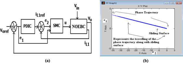
The main aim of this section is to discuss about the design of controller for NOEBC. The controller is divided into two loops namely, an inner current loop which uses SMC for control the inductor current, and an outer voltage control loop utilizing the PDIC to regulate the output voltage and steady state error of NOEBC as shown in Fig. 2(a).
|
|
|
Figure 2. Design of SMC plus PDIC, (a) the control scheme for NOEBC and (b) simulated result of region of existence of SM in the phase plane using SMC plus PDIC. |
3.1. Design of SMC
Let J be the vector which contains dynamic variables, X be the original state variables and e be the error vector.
|
|
Considered the actual state variables are x1 = iL1,x2 = Vo = Vc1, and dynamic reference variables are j1 = iL1ref,j2 = Voref. The error values e1 and e2 are expressed as (8)
|
|
(8) |
Using the phase-variable transformation to represent the NOEBC while fixing the sliding surface S(e, t), the state space average model of NOEBC in phase-variable form is expressed by (9)
|
|
(9) |
where
|
|
(10) |
For a NOEBC, the S(e, t) is defined as the linear function of tracking vector and is given by (11)
|
|
(11) |
where co-efficient vector and .
The aim of the tracking error problem is to keep the error vector (e) always on the sliding surface S(e, t) = 0, which implies that the error signal converges exponentially to zero and is engraved by (12).
|
|
(12) |
On the sliding surface, a second-order system model is reduced to first-order system model with stable linear differential equation. In addition, the system dynamics on the sliding surface is computed only by the controller co-efficient vector K. Thus, the control is insensitive to parameter variations. To calculate the control law, the error state space equation using the nearby states is derived as indicated in (13) and (14).
|
|
(13) |
|
|
(14) |
Substituting X = J–e in (14), is expressed as
|
|
(15) |
The Filippov’s average equivalent switch control ueq that guarantees the is found as
|
|
(16) |
The value of control signal is found by using the above equation and it can be expressed as
|
|
(17) |
Substituting (17) into (15) gives the system error dynamics signals as
|
|
(18) |
By applying invariance condition , the above equation is simplified as
|
|
(19) |
If exists, the vector K is derived by choosing the eigenvalues of such that it guarantees the asymptotic convergence of error to zero at the desired value. The matrix is selected to satisfy (19) and is expressed as
|
|
The values of matrix K are then found using (19) as
|
|
(20) |
Thus, the sliding surface S is given by
|
|
(21) |
Eq. (21) indicates that if the NOEBC works in sliding mode (when S = 0, stability condition), the dynamics of errors e1 and e2 be possible exponentially to zero with a time constant ratio of K1/K2. While in the step transient’s period, the NOEBC is in reaching mode, and therefore for this use K1 and K2 are computed to be in 1 and 0.09, respectively. Also (19) describes the error action under SMC. Once the sliding surface S(e, t) = Ke is designed then the control law for hitting condition is defined as
|
|
(22) |
where .
(U = 1 when the switch is the conduction subinterval, and U = 0 when the diode is the conduction subinterval).
In this work, δ = 0.05 is selected by trial and error iterative method. The (22) is applied to generate the gate pulse to drive power MOSFET of NOEBC, which in turn regulates DC output voltage, steady state error and inductor current.
In this work, M is constant number and equal to unity so that SŚ < 0 (existence condition is satisfied). The reaching condition ensures that the tracking error trajectory is asymptotically involved to S = 0 (stability condition). It is shown that Eq. (22) does not depend on the working regions, system parameters and limited disturbances. This is achieved as long as the control input u is more enough to maintain the NOEBC subsystem in sliding mode.
|
|
(23) |
where KT = [1, K2] is the vector of sliding surface coefficients which correspond to K in (17)
|
|
(24) |
After substituting the values of A, B, C and K, the above equation can be expressed by
|
|
(25) |
Equations S1(X) = 0 and S2(X) = 0 define two lines in the state plane with the same slope passing through the origin. These equations represent the sliding surface for switch ON state and OFF state conditions, which are limited to single and the sliding surface of a NOEBC with SMC for K1, K2 is shown in Fig. 2(b). From this phase trajectory, it is clearly observed that the suitable value of K2 controls the dynamic response of the system proficiently. When the phase trajectory is above the sliding surface, the switch is turned off state (U = 0) and when the phase trajectory is below the sliding surface, the switch is turned on state (U = 1).
3.2. Design of PDIC
A PIC/PDIC is selected for providing the better output voltage regulation in NOEBC. The DC output voltage is sensed and compared with reference output voltage, and error signal is obtained. This error signal is processed by the PIC/PDIC to maintain the output voltage constant and to reduce the steady state error. The PIC/PDIC parameters, proportional gain (Kp) and integral times (Ti), are obtained by using Zeigler–Nichols tuning method [16], [17], [18] and [19].
The transfer function (T.F) model of NOEBC is,
|
|
(26) |
The characteristics equation with proportional control (K) of (26) is expressed by
|
|
(27) |
The Routh array of equation (27)is
- S2: 1 K8.33e7 + 2.083e7
- S1: 666.7 − 333.3K
- S0: K8.33e7 + 2.083e7
From this Routh array, the range of K for stability is K8.33e7 + 2.083e7 > 0, K = −0.33, (666.7 − 333.3K) > 0, K > 2, 0 < K < 2. So, the ultimate critical gain Kcr = 2. When K = 2, the imaginary root since the S1 row is identically 0. The corresponding auxiliary equation is
|
|
and their corresponding roots are = 13527.7 rad/s and Pcr = 2 ∗ pi = 84954.26. After tuning the controller using this method, the NOEBC reaches expected steady state with few oscillations, where the ultimate gain for stability can be found as Kcr = 0.02 and their corresponding ultimate period as Pcr = 0.0012 s. Using this method the values of Kp = Kcr/2 = 0.01205 and integral time Ti = Pcr/.2 = 0.00133 s are determined. Also, the another value of Ti = 0.0011 is found by trial-error method based on the system performance and errors of time. The optimal values of Kp and (Ti)s of PDIC for dc output voltage regulation of NOEBC are obtained by computing the minimum values of integral of square of error (ISE), integral of time of square of error (ITAE) and integral of absolute of error (IAE) using simulation, which are listed in Table 2.
| ISE | IAE | ITAE | Kp | Tis (s) |
|---|---|---|---|---|
| 4.352e+5 | 1.347e+4 | 3.175e+6 | 0.013 | 0.0011 and 0.00133 |
The SMC plus PDIC scheme for a NOEBC converter is shown in Fig. 2(a), where the PDIC voltage controller and SMC act as outer voltage controller and inner current controller, respectively. The input to the PDIC is the output voltage error and the output sets the average reference inductor current for inner current loop. The inputs to the SMC are output voltage error e1 and the current error e2. The output of SMC u is the control signal, which in turn sets the new duty ratio of the switching pulse for driving the power MOSFET switch.
4. Simulation results and discussions
The main purpose of this section is to discuss about the simulation results of NOEBC and conventional boost converter with designed control schemes. A SMC plus PIC is used for comparison with the designed SMC plus PDIC. The validation of the system performance is done for five different conditions viz. start-up transient, line variation, load variation, steady state region and also circuit components variations. The MATLAB/Simulink simulation model is performed on the NOEBC circuits with specifications listed in Table 1.
4.1. Start-up transient
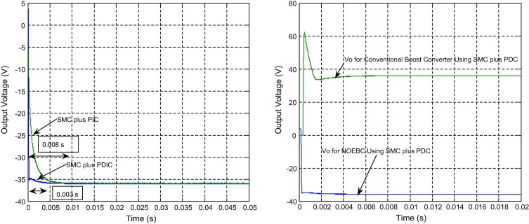
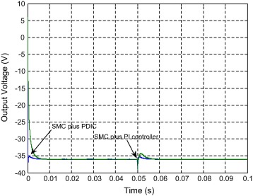
Fig. 3(a) shows the dynamic behavior in the start-up region for output voltage of NOEBC for Vin = 12 V and R = 50 Ω using both control schemes. It can be found that output voltage of NOEBC using SMC plus PDIC has a negligible overshoot and quick settling time of 0.003 s, whereas for NOEBC using SMC plus PIC there are overshoots of −0.06 V and long settling time of 0.008 s. Fig. 3(b) shows the output voltage of designed controller for both the NOEBC and conventional boost converters in start-up region. From this figure, it is clearly shown that the output voltage of NOEBC has negligible initial start-up overshoot and quick settling time over the conventional boost converter during the transient region.
|
|
|
Figure 3. (a) Simulated startup-response of average output voltage of NOEBC for Vin = 12 V with R = 50 Ω using SMC plus PDIC and SMC plus PIC and (b) Simulated response of output voltage of NOEBC and conventional boost converter using SMC plus PDIC. |
4.2. Line variation
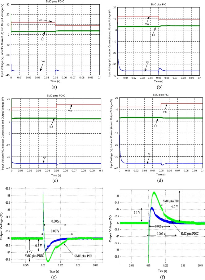
Fig. 4(a)–(d) shows the simulation responses of average output voltage and inductor current of NOEBC using both SMC plus PDIC and SMC plus PIC for input voltage step change from 12 V to 15 V and 12 V to 9 V at time of 0.05 s. Fig. 4(e) shows the distended form of response of output voltage of NOEBC for input voltage step change from 12 V to 15 V at time of 0.05 s. From this figure, it is clearly found that simulated responses of output voltage of NOEBC using SMC plus PDIC have overshoot of −0.8 V and settling time of 0.006 s, whereas for NOEBC using SMC plus PIC there are overshoot of −1.6 V and long settling time of 0.007 s. Fig. 4(f) shows the distended response of output voltage of NOEBC for input voltage step change from 12 V to 9 V at time of 0.05 s. It pinpoints that the output voltage using SMC plus PDIC has overshoot of −1.1 V and settling time of 0.006 s, while the SMC plus PIC has the overshoot of −2.5 V and long settling time of 0.007 s. From Fig. 4(a)–(d), it is well evidenced that the simulated results of the designed SMC plus PDIC exhibited an outstanding performance in comparison with a SMC plus PIC under the line variation.
|
|
|
Figure 4. Simulated responses of output voltage, inductor current and input voltage with R = 50 Ω at line variation, (a) for input step change from 12 V to 09 V at time of 0.05 s using SMC plus PDIC, (b) for input step change from 12 V to 09 V at time of 0.05 s using SMC plus PIC, (c) for input step change from 12 V to 15 V at time of 0.05 s using SMC plus PDIC, (d) for input step change from 12 V to 15 V at time of 0.05 s using SMC plus PIC, (e) Simulated response (zoomed) of output voltage of NOEBC for input step change from 12 V to 15 V at time of 0.05 s using both controllers, and (f) simulated response of output voltage of NOEBC for input step change from 12 V to 9 V at time of 0.05 s using both controllers. |
4.3. Load variation
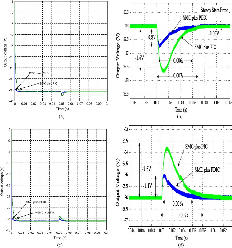
Fig. 5(a) shows the simulation response of output voltage of NOEBC using both control schemes for load step change from 50 Ω to 60 Ω at time of 0.05 s. Fig. 5(b) shows the distended response of output voltage of NOEBC. The SMC plus PDIC possesses the overshoot of −0.8 V with settling time of 0.006 s and negligible steady state error, whereas in SMC plus PIC there are overshoot of −1.6 V with long settling time of 0.007 s and steady state error of −0.06 V. Fig. 5(c) shows the simulation response of output voltage of NOEBC using both control schemes for load step change from 50 Ω to 40 Ω at time of 0.05 s. Fig. 5(d) shows the distended response of output voltage for both the cases. SMC plus PDIC has overshoot of −1.1 V with settling time of 0.006 s and negligible steady state error. The SMC plus PIC has the overshoot, the long settling time and steady state error as −2.5 V, 0.007 s and −0.06 V respectively. Fig. 5(a)–(d) proves that the designed SMC plus PDIC results in less overshoot, quick settling time and negligible steady state error in comparison with a SMC plus PIC under the load variation.
|
|
|
Figure 5. Simulated responses of output voltage of NOEBC with Vin = 12 V at load variation (a) when load value takes a step changes from 50 Ω to 60 Ω at time 0.05 s using SMC plus PDIC and SMC plus PIC, (b) zoomed output voltage when load value takes a step changes from 50 Ω to 60 Ω at time 0.05 s using SMC plus PDIC and SMC plus PIC, (c) when load value takes a step changes from 50 Ω to 40 Ω at time 0.05 s using SMC plus PDIC and SMC plus PIC, and (d) zoomed output voltage when load value takes a step changes from 50 Ω to 40 Ω at time 0.05 s using SMC plus PDIC and SMC plus PIC. |
4.4. Steady state region
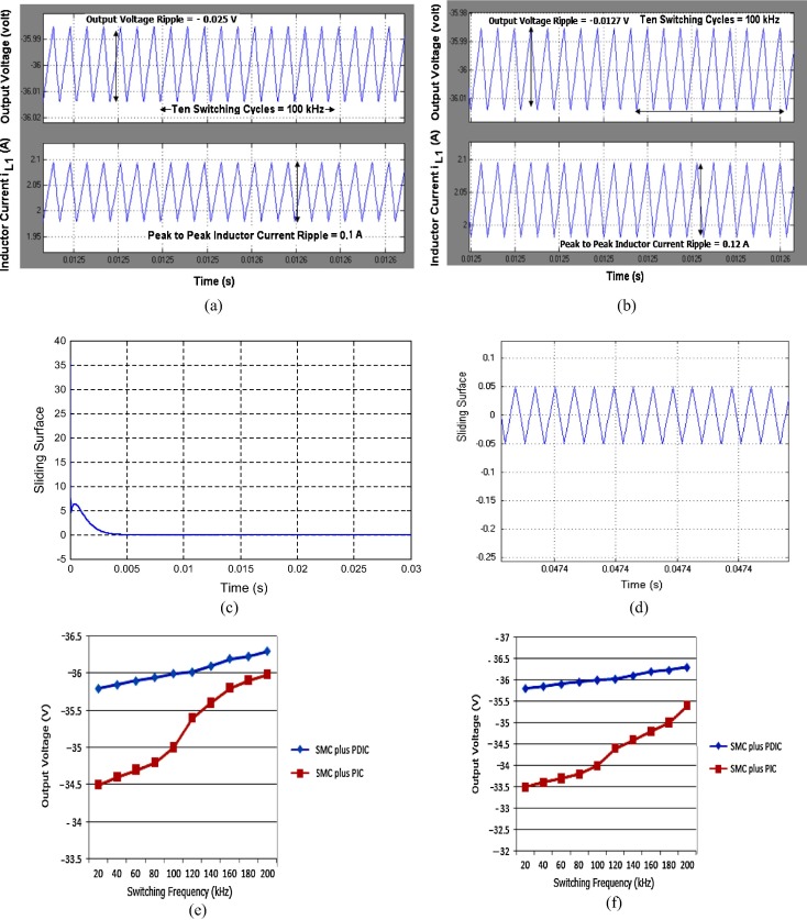
Fig. 6(a) and (b) shows the simulated instantaneous output voltage and the inductor current of NOEBC in the steady state region using both control schemes. It is evident from the figure that the output voltage ripple is very small about −0.025 V/−0.0127 V and the peak to peak inductor ripple current is 0.1 A/0.12 A for the average switching frequency of 100 kHz closer to theoretical designed value listed in Table 1. Fig. 6(c) and (d) shows the simulated response of sliding surface of NOEBC using proposed control scheme, where the sliding surface oscillates around zero. Fig. 6(e) and (f) shows the graphs of the steady-state output voltage against the switching frequency of the NOEBC under the SMC plus PDIC and SMC plus PIC respectively for the minimum and maximum output currents. From this figures, it is clearly found that the proposed controller reduces the steady-state error regulation for all values of switching frequency in comparison with SMC plus PIC.
|
|
|
Figure 6. Simulated results of NOEBC in steady state conditions, (a) output voltage and inductor current iL1 in steady state condition using SMC plus PDIC, (b) output voltage and inductor current iL1 in steady state condition using SMC plus PIC, (c) sliding surface using SMC plus PDIC at Vin = 12 V and load R = 50 Ω, (d) sliding surface in steady state condition, (e) plot of steady-state output voltage against switching frequency using both the controllers at minimum output current Io = −0.36 A, and (f) plot of steady-state output voltage against switching frequency using both the controllers at maximum output current Io = −1.8 A. |
4.5. Circuit components variations
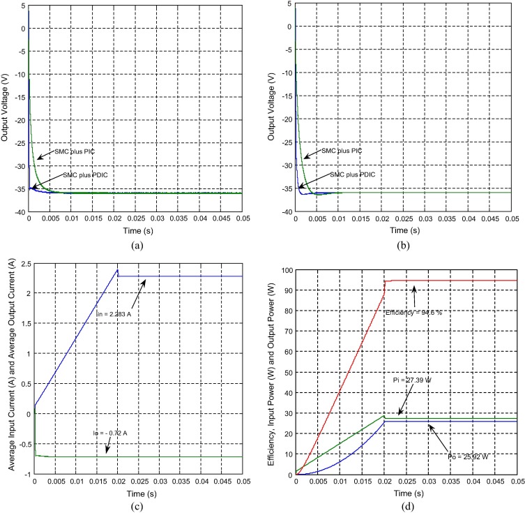
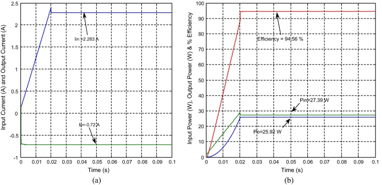
Fig. 7 shows (a) simulation response of output voltage of a NOEBC using both control schemes for the change in inductor L1 value from 100 μH to 150 μH. It could be found that the change does not influence the NOEBC behaviors due to proficient designed SMC plus PDIC in comparison with SMC plus PIC. An interesting result is illustrated in Fig. 7(b). It shows the simulation response of output voltage of a NOEBC with both control schemes for the variation in capacitor values from 30 μF to 100 μF. It can be seen that the proposed SMC plus PDIC is very successful in suppressing effect of capacitance variation except a negligible output voltage ripple and quick settling time in comparison with SMC plus PIC. From Fig. 7(c) and (d), it is evident that the average input/output currents, input/output powers and efficiency of NOEBC using proposed control scheme are 2.283 A/−0.72 A, 27.39 W/25.92 W and 94.6% respectively and match with the theoretical design presented in Table 1.
|
|
|
Figure 7. Simulated results of circuit components variation and performance of NOEBC using SMC plus PDIC, (a) output voltage when inductor variation from 100 μH to 150 μH using SMC plus PDIC and SMC plus PIC, (b) output voltage of NOEBC when inductor variation from 30 μF to 100 μF using SMC plus PDIC and SMC plus PIC, (c) average input and output currents using SMC plus PDIC, and (d) input power, output power and efficiency using SMC plus PDIC. |
5. Experimental results
The main purpose of this section is to discuss about the experimental results of NOEBC with designed SMC plus PDIC. The validation of the system performance is done for different conditions. The laboratory prototype model is performed on the NOEBC circuits with same simulation specifications. The laboratory prototype model of NOEBC using proposed control circuits is shown in Fig. 8(a). The parameters of the power circuits are as follows:
| Q | IRFN 540 (MOSFET); |
| D1 | FR306 (diodes); |
| C1 | 30 μF/100 V (electrolytic and plain polyester type); |
| L1 | 100 μH/5 A (ferrite core) |
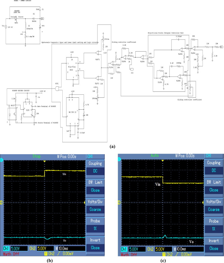
The parameters of the controller are as follows: K1 = 1, K2 = 0.09, δ = 0.05, Kp = 0.013 and Ti = 0.0011 s and 0.0013 as calculated in the previous section. The designed SMC plus PDIC is implemented in analog platform as shown in Fig. 8(a) and its operation is as follows: the inductor current and the output voltage Vo of NOEBC are sensed by using shunt resistance, and potential dividing resistances. The measured output of NOEBC is compared with reference output voltage signals by using TL084 operational amplifier, it gives the error signal, this error signal is processed through the PDIC to generate the reference current which is compared with the measured circuit inductor current and this will give the current error signal. Further, both the current and voltage errors are processed through the sliding surface coefficients and its outputs are summed to form the sliding surface using TL084 operational amplifiers. This sliding surface signals are compared using TL071 to generate the pulse width modulated (PWM) gate drive control signal. The hysteresis upper and lower limits are implemented by using the TL071, flip-flop 4013, logical AND gate, and NE 555 IC (used to generate and set the 100 kHz operating frequency for proposed system). The generated gate signal is passed through the op-isolator (6N137), driver IC 2125, and resistances and capacitor arrangement associated in the gate terminal. The output of the driver is directly connected to the gate of the MOSFET (IRFN 540) as shown in Fig. 8(a). Using the SMC plus PDIC, the switching frequency of gate pulse is varied to regulate the output voltage and inductor current and enhance the transient, reduced steady state errors and proficient dynamic performances of NOEBC.
|
|
|
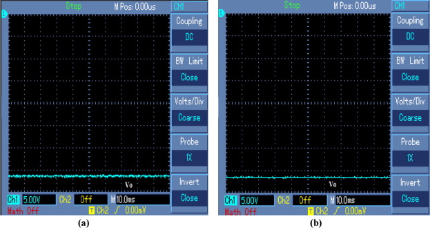
Figure 8. Experimental circuit and results of NOEBC using proposed controller at line variation, (a) Laboratory prototype model of the NOEBC using a SMC plus PDIC in analog platform, (b) output voltage of NOEBC using SMC plus PDIC for input step change from 12 V to 15 V at time 0.05 s with R = 50 Ω, and (c) output voltage of NOEBC using SMC plus PDIC for input step change from 12 V to 09 V at time 0.05 s with R = 50 Ω [Ch1:5V/Div-output voltage and Ch2:5V/Div-input voltage]. |
5.1. Line variation
Fig. 8(b) shows the experimental response of output voltage of NOEBC using SMC plus PDIC for input voltage step change from 12 V to 15 V at time of 0.05 s. From this figure, it is clearly found that experimental response of output voltage of NOEBC using SMC plus PDIC has overshoot of −1 V and settling time of 0.006 s. Fig. 8(c) shows the experimental response of output voltage of NOEBC using SMC plus PDIC for input voltage step change from 12 V to 9 V at time of 0.05 s. Experimental response of output voltage of NOEBC using SMC plus PDIC has overshoot of −1.23 V and settling time of 0.006 s.
5.2. Load variation
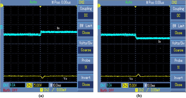
Fig. 9(a) shows the experimental response of output voltage of NOEBC using proposed control scheme for load step change from 50 Ω to 60 Ω at time of 0.05 s. It could be seen that the experimental result of output voltage of NOEBC using SMC plus PDIC has a small overshoot of −0.72 V with settling time of 0.006 s and negligible steady state error. Fig. 9(b) shows the experimental response of output voltage of NOEBC using proposed control scheme for load step change 50–40 Ω at time of 0.05 s. It could be seen that the experimental result of output voltage of NOEBC using SMC plus PDIC has a small overshoot of −0.88 V with settling time of 0.006 s and negligible steady state error.
|
|
|
Figure 9. Experimental results of NOEBC using proposed controller at load variation (a) output voltage of NOEBC using SMC plus PDIC for load step change from 50 Ω to 60 Ω at time 0.05 s with Vin = 12 V and (b) output voltage of NOEBC using SMC plus PDIC for load step change from 50 Ω to 40 Ω at time 0.05 s with Vin = 12 V [Ch1:1A/Div-output voltage and Ch2:5V/Div-input voltage]. |
5.3. Circuit components variation
Fig. 10 shows (a) experimental response of output voltage of a NOEBC using proposed controller for inductor L1 variation from 100 μH to 150 μH. It could be found that the change does not influence the NOEBC behaviors due to proficient designed SMC plus PDIC. An interesting result is illustrated in Fig. 10(b). It shows the experimental response of output voltage of a NOEBC using SMC plus PDIC for the variation in capacitor values from 30 μF to 100 μF. From these figures it is clearly found that the proposed SMC plus PDIC is very successful in suppressing effect of capacitance variation except a negligible output voltage ripple and quick settling time.
|
|
|
Figure 10. Experimental output voltage response of circuit components variation of NOEBC using SMC plus PDIC (a) for inductor variation from 100 μH to 150 μH and (b) for capacitor variation from 30 μF to 100 μF. |
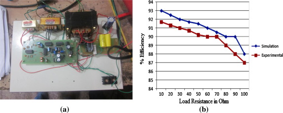
Fig. 11(a) indicates the photograph of laboratory prototype set-up model of NOEBC using designed controller. Fig. 11(b) indicates that simulation and experimental results of percentage efficiency of NOEBC using SMC plus PDIC at various load conditions. The efficiency of NOEBC using SMC plus PDIC is improved from 87% to 93% at various load conditions.
|
|
|
Figure 11. Photograph model and performance of NOEBC using SMC plus PDIC, (a) photograph of laboratory prototype set-up model and (b) simulation and experimental results of % efficiency at various load conditions. |
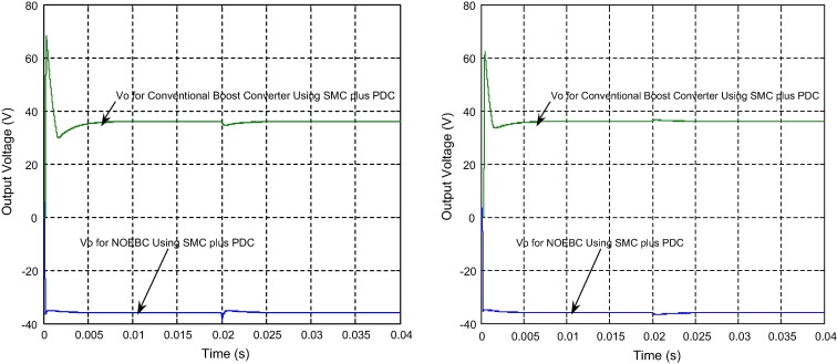
Fig. 12(a) shows the output voltage of designed controller for both the NOEBC and conventional boost converters when input supply voltage varied from 12 V to 15 V. From this figure, it is clearly shown that the output voltage of NOEBC has better performance over the conventional boost converter during line variation region. Fig. 12(b) shows the output voltage of designed controller for both the NOEBC and conventional boost converters when load resistance varied from 50 Ω to 60 Ω. From this figure, it is clearly shown that the output voltage of NOEBC has excellent performance in comparison with the conventional boost converter under the load variation region.
|
|
|
Figure 12. Simulated output voltage of NOEBC and conventional boost converter using SMC plus PDIC, (a) input supply voltage variation from 12 V to 15 V at time of 0.02 s and (b) load resistance variation from 50 Ω to 60 Ω. |
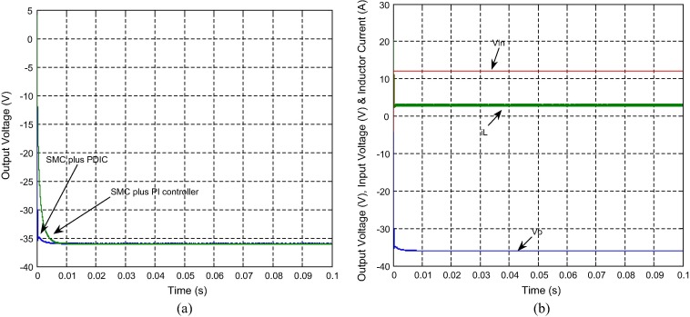
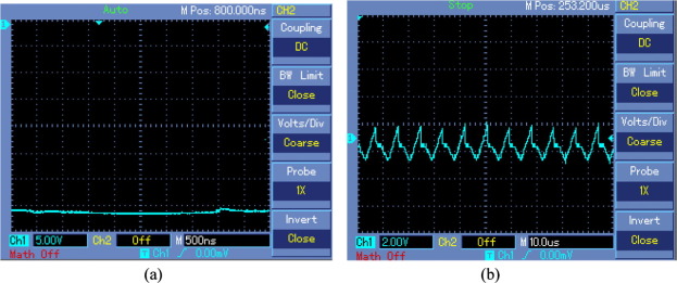
Fig. 13(a) shows the simulated output voltage response of the NOEBC with inductive load (R = 50 Ω and L = 10 μH) using both controllers in transient state with nominal power ratings. From this result, it is evident that the output voltage of the same converter using designed controller has quick settling time and negligible overshoot over the SMC plus PI controller with inductive load. Fig. 13(b) shows the simulated inductor current, input voltage and output voltage of the NOEBC using SMC plus PDIC. It can be found that the output voltage of this converter has negligible overshoot, whereas the inductor current of same converter using controller has produced small overshoot in transient region with inductive load. Fig. 14(a) shows the simulated average input and output currents of the NOEBC with inductive load using SMC plus PDIC. It is evident that the average output current and input current of NOEBC exactly match the theoretical value. Fig. 14(b) shows the simulated performance of the NOEBC using designed controller with inductive load. From these results, it is clearly focused that the efficiency of this converter has slightly higher (94.56%) for inductive load in comparison with resistive load. Fig. 15 shows the simulated output voltage of the converter using both controllers for input voltage variation with inductive load. It can be seen that the output voltage of the converter has produced less steady state error, small overshoot and quick settling time using designed controller in comparison with PI controller. Fig. 16 shows (a) experimental output voltage response of the NOEBC using designed controller for line variation (12–09 V) with inductive load. It is found that the output voltage has small overshoot and quick settling time using SMC plus PDIC with inductive load. Fig. 16(b) shows the experimental sliding surface of SMC plus PDIC for NOEBC.
|
|
|
Figure 13. Simulated results of NOEBC with inductive load (R = 50 Ω and L = 10 μH) using both the controllers in transient region, (a) output voltage and (b) input voltage, inductor current and output voltage. |
|
|
|
Figure 14. Simulated results of NOEBC with inductive load (R = 50 Ω and L = 10 μH) using SMC plus PDIC, (a) average input and output currents and (b) input power, output power and efficiency. |
|
|
|
Figure 15. Simulated output voltage results of NOEBC with inductive load (R = 50 Ω and L = 10 μH) using both the controllers in line variations (12–09 V). |
|
|
|
Figure 16. Experimental results of NOEBC with inductive load (R = 50 Ω and L = 10 μH) using the controllers in line variations (12–09 V), (a) output voltage (input voltage variation) and (b) sliding surface. |
In summary, from Figure 3, Figure 4, Figure 5, Figure 6, Figure 7, Figure 8, Figure 9, Figure 10, Figure 11, Figure 12, Figure 13, Figure 14, Figure 15 and Figure 16, it is clearly indicated that the experimental results of the NOEBC using the designed SMC plus PDIC match the simulated results with a tolerance of ±2.5%. Finally, the proposed SMC plus PDIC performed well in the entire operating situation of the NOEBC.
6. Conclusions
In this article, the theoretical analysis, design, and output voltage regulation of the NOEBC operated in CCM using a variable frequency based SMC plus PDIC have been successfully demonstrated. The proposed controller parameters have been implemented in analog platform. A major merit over a linear PIC lies in the fact that the SMC plus PDIC is robust to large variations on line, load and parameter variations without modifying the sliding coefficients. Many simulation and experimental results are presented in order to prove the performance of the proposed controller. The influence of the controller parameters on the performances of the system is studied.
The effortless analog circuit based implementation of a SMC plus PDIC and detailed experimental analysis are the key contributions of this article. Theoretical analysis, experimental and simulations are presented to illustrate the effectiveness of designed SMC plus PDIC for the NOEBC operated in CCM with resistive and inductive loads resulted in fast dynamic response, proficient regulated output voltage, non-disturbed output voltage during the circuit component variations, excellent steady state and transient responses, etc. Also, the simulation results of NOEBC using designed controller have better performance in comparison with conventional boost converter using the same controller. It is, therefore, suitable for any stable power source real-world commercial applications and it is mainly designed for power supply in different medical equipments, telecom, industrial and military applications.
References
- [1] O. Abutbuli, A. Gherlitz, Y. Berkovich, A. Ioinovici; Step-up switching-mode converter with high voltage gain using a switched-capacitor circuit; IEEE Trans. Circuits Syst. I, 50 (8) (2003), pp. 1098–1102
- [2] C. Tseng, T.J. Liang; Novel high-efficiency step-up converter; IEE Proc. Electr. Power Appl., 151 (2) (2004), pp. 182–190
- [3] http://www.researchandmarkets.com.
- [4] D.D.C. Lu, D.K.W. Cheng, Y.S. Lee; A single-switch continuous conduction-mode boost converter with reduced reverse-recovery and switching losses; IEEE Trans. Ind. Electron., 50 (4) (2003), pp. 767–776
- [5] L.S. Yang, T.J. Liang, J.F. Chen; Transformer less DC–DC converters with high step-up voltage gain; IEEE Trans. Ind. Electron., 56 (8) (2009), pp. 3144–3152
- [6] B. Bryant, M.K. Kazimierczuk; Voltage-loop power-stage transfer functions with MOSFET delay for boost PWM converter operating in CCM; IEEE Trans. Ind. Electron., 54 (1) (2007), pp. 347–353
- [7] J.A. Abu Qahouq, H. Mao, H. Zhou, I. Batarseh; DC–DC converter with interleaved current doublers and parallel connected transformers scheme; IET Power Electron., 1 (1) (2008), pp. 27–37
- [8] M. Zhu, F.L. Luo; Implementing of developed voltage lift technique on SEPIC, CUK and double-output DC–DC converters; IEEE Trans. Ind. Electron. Appl., 23 (25) (2007), pp. 674–681
- [9] F.L. Luo, H. Ye; Negative output cascade boost converters; IEE Proc. Electr. Power Appl., 151 (5) (2004), pp. 590–606
- [10] F.-L. Luo, Hong Ye; Advanced DC/DC Converters; CRC Press, London (2006)
- [11] Viera Biolkova, Zdenek Kolka, Dalibor Biolek; State-space averaging (SSA) revisited: on the accuracy of SSA-based line-to-output frequency responses of switched DC–DC converters; WSEAS Trans. Circuits Syst., 9 (2) (2010), pp. 81–90
- [12] Asma Merdassi, Laurent Gerbaud, Seddik Bacha; Automatic generation of average models for power electronics systems in VHDL-AMS and modelica modelling languages; J. Modell. Simulat. Syst., 1 (3) (2010), pp. 176–186
- [13] R. Middlebrook, S. Cuk; A general unified approach to modeling switching-converter power stages; Int. J. Electron., 42 (6) (1977), pp. 521–550
- [14] M. Veerachary; General rules for signal flow graph modeling and analysis of dc–dc converters; IEEE Trans. Aerosp. Electron. Syst., 40 (1) (2004), pp. 259–271
- [15] P. Mattavelli, L. Rossetto, G. Spiazzi; Small signal analysis of DC–DC converter with sliding mode control; IEEE Trans. Power Electron., 12 (1) (1997), pp. 96–102
- [16] A.J. Forsyth, S.V. Mollow; Modelling and control of DC–DC converters; Power Eng. J., 12 (5) (1998), pp. 229–236
- [17] P. Comines, N. Munro; PID controllers: recent tuning methods and design to specification; IEEE Proc. Control Theory Appl., 149 (1) (2002), pp. 46–53
- [18] H. Sira-Ramirez; On the generalized PI sliding mode control of DC-to-DC power converters: a tutorial; Int. J. Control, 76 (9/10) (2003), pp. 1010–1033
- [19] Katshika Ogata; Modern Control Engineering; (third ed.)Prentice–Hall of India Private Limited, New Delhi (1997)
- [20] J.J.E. Slotine, W. Li; Applied Nonlinear Control; Prentice-Hall, Englewood Cliffs, NJ (1991)
- [21] R.A. De Carlo, S.H. Zak, G.P. Matthews; Variable structure control of nonlinear multivariable systems: a tutorial; Proc. IEEE, 76 (1988), pp. 212–234
- [22] I. Utkin; Sliding Mode and Their Application in Variable Structure Systems; U.S.S.R. MIR, Moscow (1978)
- [23] Siw-Chong Tan, Y.M. Lai, C.K. Tse; General design issues of sliding-mode controllers in DC–DC converters; IEEE Trans. Ind. Electron., 55 (3) (2008), pp. 1160–1174
- [24] Yiwen Hey, Weisheng Xu, Yan Cheng; A novel scheme for sliding mode control of DC–DC converter with a constant frequency based on the averaging model; J. Power Electron., 10 (1) (2010), pp. 1–8
- [25] L. Martinez-Salamero, A. Cid-Pastor, R. Giral, J. Calvente, V. Utkin; Why is sliding mode control methodology needed for power converters?, Proceedings of 14th International Power Electronics and Motion Control Conference (Short Form of the Conference) (2010) S9-25–S9-31
- [26] S.-C. Tan, Y.-M. Lai, Chi K. Tse, Luis Martneiz Slamero, Chi-Kin Wu; A fast response sliding mode controller for boost type converter with a wide range of operating condition; IEEE Trans. Ind. Electron., 54 (6) (2007), pp. 3276–3286
- [27] Leopoldo Rossetto, Giorogio Spiazzi; Fast-response high-quality rectifier with sliding model control; IEEE Trans. Power Electron., 9 (1994), pp. 46–152
- [28] S.-C. Tan, Y.-M. Lai, M.-K.-H. Cheung, C.-K. Tse; On the practical design of a sliding mode voltage controlled buck converter; IEEE Trans. Power Electron., 20 (2) (2005), pp. 425–437
- [29] H. Sira-Ramirez, M. Rios-Bolivar; Sliding mode control of DC-to-DC power converters via extended linearization; IEEE Trans. Circuits Syst. I, Fundam. Theory Appl., 41 (10) (1994), pp. 652–666
- [30] Y. Jiao, F.-L. Luo, M. Zhu; Generalized modeling and sliding mode control for n-cell cascade super-lift DC–DC converters; IET Power Electron., 4 (5) (2011), pp. 532–540
- [31] RaḿOn O. ĆAceres, Ivo Barbi; A boost DC–AC converter: analysis, design, and experimentation; IEEE Trans. Power Electron., 14 (1) (1999), pp. 134–141
- [32] M.G. Umamaheswari, G. Uma, K.M. Vijayalakshmi; Design and implementation of reduced-order sliding mode controller for higher-order power factor correction converters; IET Power Electron., 4 (9) (2011), pp. 984–992
- [33] K. Ramash Kumar, S. Jeevananthan; Modelling and implementation of fixed switching frequency sliding mode controller for negative output elementary super lift Luo-converter; IET Power Electron., 5 (8) (2012), pp. 1593–1604
- [34] Kuppan Ramash Kumar, Seenithangam Jeevananthan; Sliding mode control for current distribution control in paralleled positive output elementary super lift Luo converters; J. Power Electron., 11 (5) (2011), pp. 639–654
- [35] K. Ramash Kumar, S. Jeevananthan; A sliding mode control for positive output elementary Luo converter; J. Electr. Eng., 10 (4) (2010), pp. 115–127
- [36] Y. He, F.L. Luo; Study of sliding mode control for dc–dc converters, International Conference on Power System Technology (POWERCON 2004), Singapore (2004), pp. 1969–1974
- [37] J. Mahdavi, A. Emadi, H.A. Toliyat, Application of state space averaging method to sliding mode control for PWM DC/DC converters, IEEE Industry Application Society Annual Meeting, New Orieans, Louisianan, 1997, pp. 820–827.
- [38] S.C. Tan, Y.M. Lai, C.K. Tse; Indirect sliding mode control of power converters via double integral sliding surface; IEEE Trans. Power Electron., 23 (2) (2008), pp. 600–611
- [39] N. Li, X. Lin-Shi, P. Lefranc, E. Godoy, A. Jaafar; FPGA based double-integral type of indirect sliding mode control for high frequency single-ended primary inductor converter; ISIE, Gdansk, Poland (2011) http://dx.doi.org/10.1109/ISIE.2011.5984395
- [40] N. Arunkumar, T.S. Sivakumaran, K. Ramash Kumar, S. Saranya; Reduced order linear quadratic regulator plus proportional double integral based controller for a positive output elementary super lift Luo converter; J. Theor. Appl. Inf. Technol., 65 (3) (2014), pp. 890–901
Document information
Published on 12/04/17
Licence: Other
Share this document
Keywords
claim authorship
Are you one of the authors of this document?

