- Correction added on 26 July 2016, after first online publication: This article was edited after first online publication.
Abstract
An Al2O3/TiO2 double layer anti-reflection coating (ARC) film formed by spray pyrolysis was introduced for monocrystalline silicon solar cells as the nonvacuum processing method. The thickness of the Al2O3 layer and TiO2 compact layer was controlled by the volume of deposited precursor solution and confirmed by ellipsometry and scanning electron microscopy. The average photovoltaic properties of photocurrent density (Jsc), open-circuit photovoltage (Voc), fill factor (FF), and photo energy conversion efficiency (η) were 37.0 mA/cm2, 590 mV, 0.712, and 15.5%, respectively. A significant improvement on Jsc and η could be confirmed owing to the Al2O3/TiO2 ARC. The results of Fourier transform infrared (FTIR) spectroscopy and optical simulation with modeling for the reflectance properties confirmed that C-H-based organics remained after the deposition of thin films.
Introduction
Reducing optical losses in solar cells is a major factor for achieving high-efficiency silicon solar cells, and improving the absorption properties is one of the key features counteracting such loss. Various materials and thin films, including SiO2, SiNx, TiO2, Al2O3, etc., have been used for anti-reflection coating (ARC) purposes depending on the type of solar cells.
In earlier decades, TiO2 was introduced as an anti-reflection layer for crystalline silicon solar cells [1, 2], due to its good optical properties that enhance light absorption capability, and because of the high refractive index for silicon solar cells. Today, SiNx has dominated the silicon solar cell industry, due to even better optical characteristics and a passivation effect which leads to high bulk lifetimes [3, 4]. SiNx or the stack layers (e.g. SiNx/SiOx) are deposited by a well-known plasma-enhanced chemical vapor deposition technique [5, 6]. However, the needs for vacuum processing of toxic and hazardous gases such as SiH4 and NH3 in CVD operation are major drawbacks, due to the considerable costs involved.
In order to meet industrial requirements with simple low-cost technologies, high-throughput, cost-effective methods need to be investigated and adapted to the solar cell manufacturing process. A considerable amount of literature has been published on sol–gel processes including TiO2, TiO2-SiO2 [1, 7], and some Al2O3-based Ti-doped mixed sol–gel sources as well [8, 9]. However, further investigations are needed to apply these kinds of low-cost materials to the solar cell fabrication processes.
In this work, as a low temperature and nonvacuum method, spray-pyrolysis deposition was performed for TiO2 layer and Al2O3 layers, and the Al2O3/TiO2 double layer was introduced as an alternative anti-reflection coating film. Film structures were modeled and confirmed by experimental studies. Applying appropriate film thicknesses for each layer and the suitable order of the layers according to their refractive indexes are the key points [10, 11]. From that point of view, after confirming the structure of TiO2 and Al2O3 thin films separately, <air/Al2O3/TiO2/Si> double layer structure was built considering the gradual increasing order of refractive indexes – 1.7, 2.3, 4.3 – for Al2O3, TiO2, and silicon, respectively, where the refractive index of air is equal to 1. Owing to the advantage of this gradual increase in refractive index on the light path, much lower reflectance can be expected [10, 11]. Finally, silicon solar cells were fabricated with and without using Al2O3/TiO2 double coating film.
Experimental
At first, TiO2 and Al2O3 films were formed on flat crystalline silicon substrates and primary evaluation of the coating films was carried out. After optical optimizations, Al2O3/TiO2 double layer anti-reflection coating films were applied to the silicon solar cells fabricated on textured wafers.
For the optical measurements, square-shaped p-type Si wafers (25 × 25 mm2) were cut out from 6-inch Cz-Si p-type wafers. All wafers were processed by HF dip (20 v/v %) for 1 min and DI (deionized) water rinse. UV/O3 surface treatment was carried out for a complete cleaning process. TiO2 and Al2O3 films were formed on the silicon wafers by spray pyrolysis deposition using precursor solutions which were sprayed on to the surface of silicon wafers using a glass atomizer. The Si wafers were set on a hot plate heated at a deposition temperature of 450°C. The TiO2 precursor solution was prepared by 10-fold dilution of titanium bis-isopropoxidebis-acethylacetone (TAA) (prepared by mixing titanium (VI) isopropoxide and acetylacetone in a 1:2 mole ratio) to ethanol. The Al2O3 precursor solution was 0.03 mole L−1 of aluminum (III) acetylacetonate (Al(acac)3) in ethanol solution. Deposited film thicknesses were mainly controlled by the amount of sprayed precursor solutions. Each layer was analyzed by an ellipsometer (Uvisel ER Agms-nsd, HORIBA, Ltd., Kyoto, Japan).
Fittings of ellipsometer spectrum were performed by DeltaPsi2 software, using Horiba Jobin Yvon, Uvisel ErAgms-nds, considering the rough structures and the mixtures with organic residues. Scanning electron microscope (SEM) measurements (JSM-6510, JEOL), reflection analysis by ultraviolet–visible spectroscopy (Lambda 750 UV/VIS Spectrometer; Perkin Elmer, Waltham, Massachusetts, USA), and Fourier transform infrared spectroscopy (FTIR) (Frontier FTIR, Perkin-Elmer) were performed for the analysis.
Silicon solar cells were fabricated in four different sets with a variety of surface conditions: with/without ARC on the silicon surface, with/without texture. For the fabrication of silicon solar cells, 25 ×25 mm p-type Cz-Si wafers were used, which were also cut out from 6-inch wafers. For surface-textured Si solar cells, alkaline texturing was performed in KOH (5.19 g) solution in H2O (100 mL) with Alka-Tex (GP Solar [Hainbuchenring, Neuried, Germany]; 0.28 mL) at 80°C (set: 100°C) for 30 min. In order to prevent texturing the the back side of the Si wafer was coated with polysilazane by a spin coater twice at 1500 rpm for 20 sec, followed by annealing at 600°C for 60 min in O2 gas flow. The Si wafers were processed by HF dip (20 v/v %) for 10 min and DI water rinse. RCA cleaning [12] was then carried out to remove contaminant particles on the surface of the wafers using a NH4OH/H2O2/H2O (1:1:5 in volume) solution, for 10 min at 80°C. After removal of the natural oxide films by HF dip (20 v/v %), a mixed solution of HCl/H2O2/H2O (1:1:5 in volume) was used to remove metallic contaminations and mobile ions on the surface by dipping the wafers for 10 min at 80°C. In order to prevent phosphorous diffusion on the back side of the Si wafer, silicon dioxide layer was formed on the back side using precursor solution (polysilazane) which was coated by a spin coater twice at 1500 rpm for 20 sec, followed by annealing at 600°C for 60 min in O2 gas flow. For n+-emitter formation, POCl3 diffusion was performed at 880°C for 40 min with 0.2 Lmin−1 N2 flow. Afterward, the wafers were treated with an HF dip (10 v/v %) and a DI water rinse, successively. Front and back contacts were formed by screen-printing Ag and Al, respectively. Screen-printed pastes were dried at 125°C for 5 min (the dried Al paste was ca. 40 μm thick) and co-firing was carried out at 800°C for 1 min in an oven. After optimization by optical analysis, a double layer ARC film was formed with a 90 nm Al2O3 film over a 40 nm TiO2 film using 100 and 4 mL precursor solutions, respectively.
Results and Discussion
Evaluation of thin films
In order to analyze and optimize TiO2 and Al2O3 spray on deposited layers for the processing of Al2O3/TiO2 double layer film, single-layered TiO2 and Al2O3 films were analyzed. The fitting models were considered for the simulation. First, a fitting model with a “flat layer (main body of the layer)” and a “roughness layer (surface residue)” was defined according to the SEM images depicted in Figure 1A, named as “Fitting Model #1.” It was then improved by considering “organic elements” in the roughness layer, shown in Figure 1B, named as “Fitting model #2.” The “organic elements” was a parameter in the fitting software of the ellipsometer (Horiba Jobin Yvon, Uvisel ErAgms-nds).
|
|
|
Figure 1. (A) Example of a scanning electron microscope (SEM) image; (B) Fitting Model #1 consists of a “flat layer” and a “roughness layer”; (C) Fitting Model #2 consists of a “flat layer” and a “roughness layer containing organic elements.” |
Tables 1 and 2 show the fitting results of 60 mL TiO2 and 100 mL Al2O3 precursor deposited on Si wafer, respectively, using the models in Figure 1. “Matching factor” stands for the perfectness of the fitting between the experimental data and the fitting data, which is expected to be below “1” for a good matching [13]. “Void” and “organic” in the material ratio column and the rough-layer line show the percentage of air and organic material in the rough layer, respectively. Hydrocarbon-based organics can remain inside the formed layer due to organics contained in the precursor solution. The difference between Fitting Models #1 and #2 is the presence and absence of “organic” elements in the rough layer. Owing to the organics, the matching factor of the TiO2 film and Al2O3 film decreased significantly from 6.88 to 0.251 and from 2.79 to 0.346, respectively, resulting in a significantly more reliable fitting for the estimation of film thickness of sprayed TiO2 and Al2O3 in this work. TiO2 film was occupied by a flat layer of 84.2%. On the other hand, Al2O3 film was occupied by a rough layer of 93.3%.
| Fitting Model #1 | Fitting Model #2 | |||
|---|---|---|---|---|
| Thickness/nm | Material ratio | Thickness/nm | Material ratio | |
| Flat layer | 60.1 | TiO2 (100%) | 54.4 | TiO2 (100%) |
| Roughness layer | 2.16 | TiO2 (31.7%)/void (68.3%) | 10.2 | TiO2 (33.4%)/void (25.5%)/organic (36.1%) |
| Matching factor | 6.88 | 0.251 | ||
| Fitting Model #1 | Fitting Model #2 | |||
|---|---|---|---|---|
| Thickness/nm | Material ratio | Thickness/nm | Material ratio | |
| Flat layer | 11.3 | Al2O3 (100%) | 5.28 | Al2O3 (100%) |
| layer | 66.6 | Al2O3 (81.3%)/void (18.7%) | 73.3 | Al2O3 (71.54%)/void (11.45%) /organic (17.03%) |
| Matching factor | 2.79 | 0.346 | ||
For further investigation, FTIR spectra of deposited thin films were measured in a wide spectrum from 400 to 4000/cm to analyze optical film properties. Figures 2A and B show the FTIR spectra of single-layer TiO2/Si and Al2O3/Si structures after spray pyrolysis deposition, respectively. Hydrocarbon-based organic peaks were observed at 2850, 2866.3, 2929.9 and 2967/cm in the FTIR spectra of TiO2 films formed on silicon wafers. These multiple peaks from 2850 to 2970/cm can be assigned to C–H absorptions including CH2 and CH3-based compounds [14] which show the presence of organics. Similar peaks at 2851.3, 2865.8, 2928.3 and 2964/cm were also observed in Al2O3 films formed on silicon substrates.
|
|
|
Figure 2. TiO2 (A) and Al2O3 (B) films formed on Si substrate by the spray pyrolysis deposition method. |
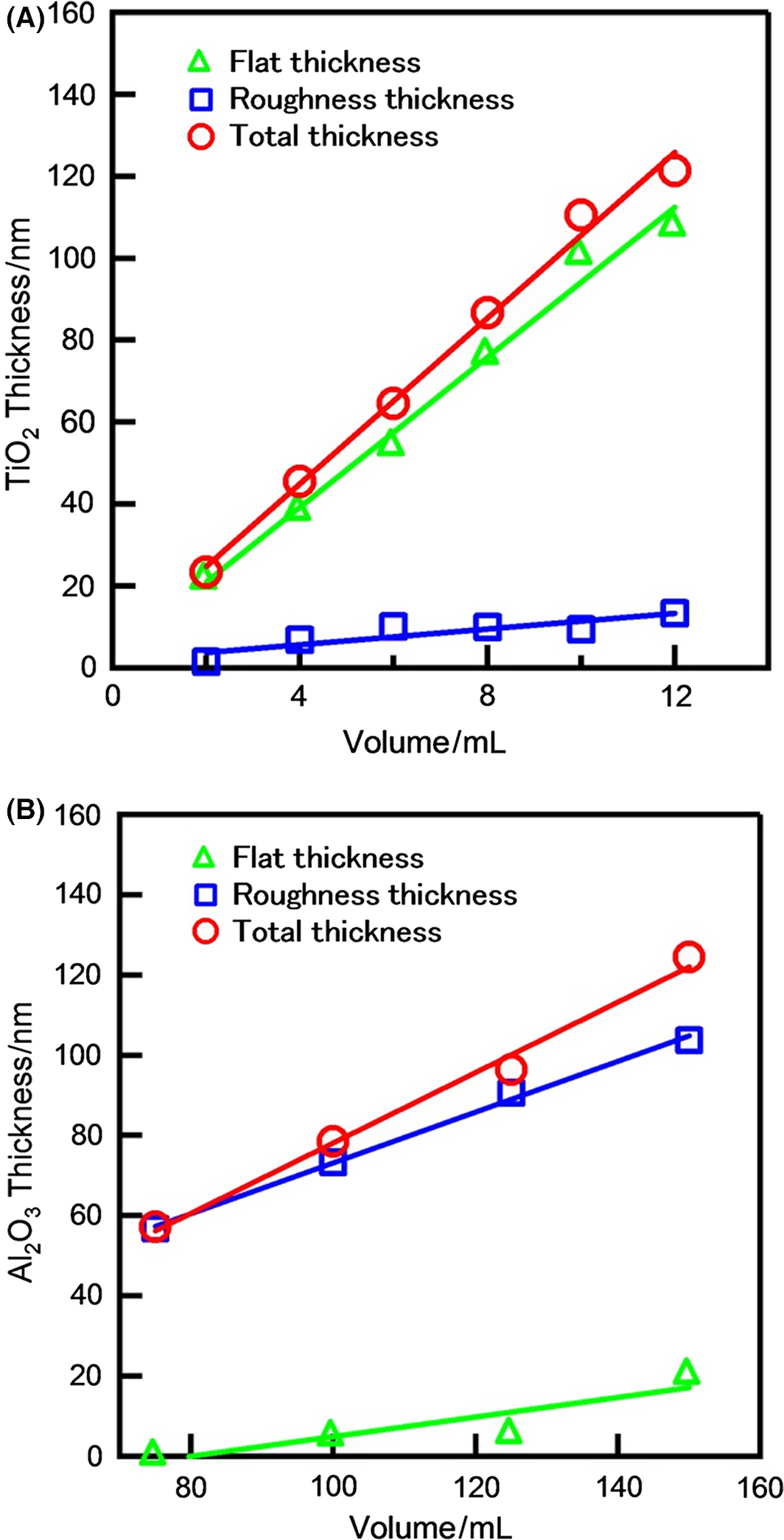
Furthermore, dependences of the TiO2 and Al2O3 film thicknesses including flat and rough layers were estimated by changing the deposition volume of the precursor solution based on ellipsometry measurements. Figures 3A and B present the estimated thickness data of TiO2 and Al2O3 films, respectively. Total thickness was calculated by the sum of rough and flat layers. According to these results, deposition rates of TiO2 and Al2O3 films can be calculated as 10.1 nm mL−1 and 0.88 nm mL−1, respectively.
|
|
|
Figure 3. TiO2 (A) and Al2O3 (B) films formed by changing the amount of precursor solutions. |
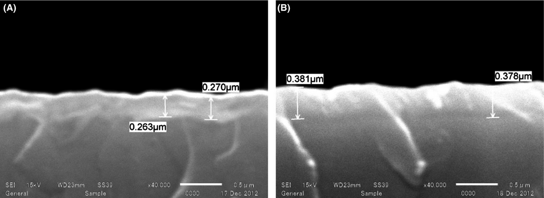
In order to confirm the deposition speed, the cross-sectional SEM images were also observed as shown in Figure 4 using thick TiO2 and Al2O3 films. TiO2/Si (Fig. 4A), and Al2O3/Si (Fig. 4B) structures formed by spray pyrolysis depositions using 30 mL TiO2 and 400 mL Al2O3 precursor solutions had approximately film thicknesses of 260 and 380 nm, respectively, according to the images. Based on these values, the deposition rates can be calculated as 8.7 nm mL−1 for TiO2 and 0.95 nm mL−1 for Al2O3 films. However, according to the ellipsometer measurements, deposition rates were found as 10.1 nm mL−1 for TiO2 deposition and 0.88 nm mL−1 for Al2O3 deposition. This difference may be attributed to the effect of surface residue and roughness after deposition when the deposition is a considerably thicker layer.
|
|
|
Figure 4. (A) 30 mL TiO2 precursor solution layer on silicon substrate; (B) 400 mL Al2O3 precursor solution layer. Each layer was deposited by the spray pyrolysis deposition method. |
For the optimization process of <Al2O3/TiO2> double layer, the thickness of the TiO2 film was varied between 20 and 120 nm (precursor solution 2–12 mL) while the thickness of the Al2O3 film was changed from 68 to 135 nm (precursor solution 75–150 mL).
After the reflectance measurements of the cells with ARC, maximal short circuit current densities from the reflectance results were calculated using equation (1) in order to observe the optimum Al2O3 and TiO2 film thicknesses to obtain efficient Al2O3/TiO2 double layer ARC film.
|
|
(1) |
where “Jsc,max” is the maximum short circuit current density from the reflectance results in mA cm−2, “e” stands for the charge of an electron (1.602 × 10⁻¹⁹ C), “h” is Plancks constant (6.626 × 10⁻³⁴ J s−1), “c” is the speed of light (2.998 × 10⁸ m s−1), “Pin” is the input power of solar irradiation (AM1.5, W (m2 nm)−1), and “λ” is the wavelength in nm.
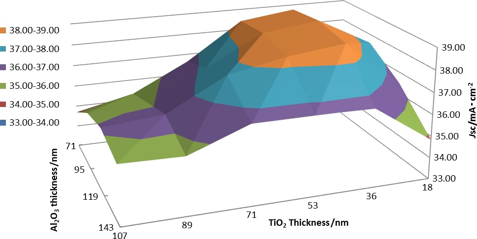
Figure 5 presents the short circuit current density (Jsc,max) calculated by equation (1) using experimental reflectance spectra of silicon substrate with Al2O3/TiO2 ARC film for various thicknesses of Al2O3 and TiO2 films. According to the calculations using experimental absorption spectra, the maximum value of Jsc,max of 38.9 mA cm−2 was achieved with a 90 nm Al2O3/40 nm TiO2 double layer ARC film (data not shown). Based on the experimental finding, the 90 nm Al2O3/40 nm TiO2 double layer ARC film was applied when fabricating silicon solar cells.
|
|
|
Figure 5. Estimated Jsc calculated by the experimental reflectivity data using <Al2O3/TiO2/Si> layers with various thicknesses of Al2O3 and TiO2 films. |
Solar cells with Al2O3/TiO2 ARC film
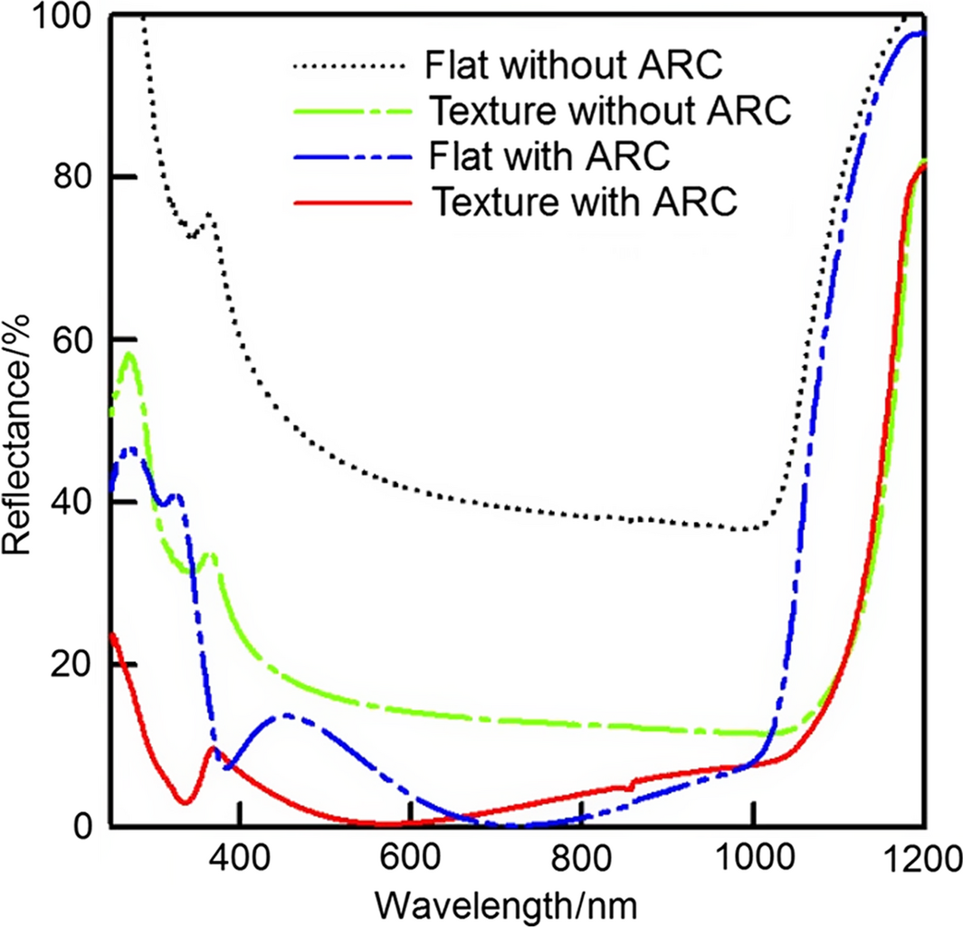
Reflectivity measurements of four types of surfaces (with/without ARC, with/without texture) are given in Figure 6. The average reflectivity of the flat silicon surface without ARC was around 40% and decreased to around 20% after texturing. By applying the double layer ARC film on the flat and textured silicon surfaces, the reflectivity was decreased significantly to a minimum of 0.2% at around 700 nm and to 0.4% at around 600 nm, respectively. As a result, the average reflectance values with the ARC on flat and textured Si surfaces were 20.1% and 9.71%, respectively. In reference also, additional increase in JSC can be expected by texture [15].
|
|
|
Figure 6. Reflectance spectra of silicon wafers with various surface structures. |
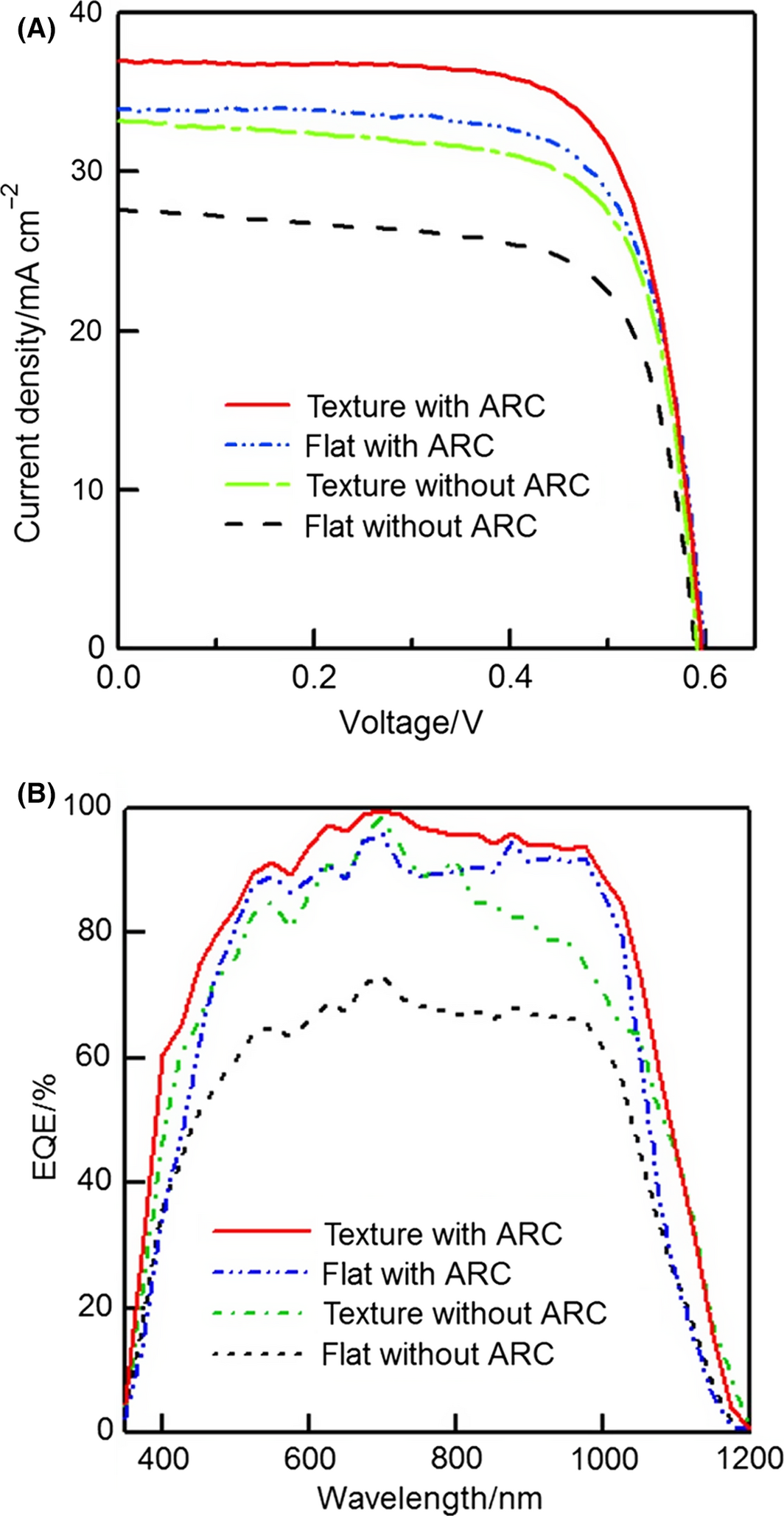
The electrical characteristics of fabricated solar cells shown in Figure 7 are summarized in Table 3. Owing to the double layer ARC film, JSC of the solar cells improved remarkably. Without ARC, JSC of solar cells with flat surface was around 27.6 mA cm−2 where it improved up to 33.5 mA cm−2 by texturing. The average JSC of the flat cells with Al2O3/TiO2 double layer ARC was 34.3 mA cm−2, which improved to 37.0 mA cm−2 by the textured silicon cell with Al2O3/TiO2 double layer ARC. Consequently, the Cz-Si p-type solar cells with Al2O3/TiO2 double layer ARC on textured surface reached a η of 15.5% with a VOC of 590 mV and FF of 71.2. A significant improvement on JSC and η could be confirmed owing to the Al2O3/TiO2 ARC when compared to the textured cells without ARC. The increase in JSC was related to the suppression of reflectance (Fig. 6) and the improvement of external quantum efficiency (EQE) (Fig. 7B), clearly. At short wavelength in Figure 7B, EQE was suppressed especially under 400 nm may be due to the absorption of the TiO2 layer which has a high extinction coefficient at short wavelength. The small fluctuation in the range of 500–1000 nm could be due to measurement error. It is well known that the passivation effect of TiO2 would be degraded by annealing over 350°C, which affects the decrease in carrier lifetime and open circuit voltage [16, 17]. Therefore, another passivation layer like a silicon dioxide should be inserted between silicon and TiO2 to achieve higher open circuit voltage, which is a future subject of study in our group. We have also confirmed the calculated JSC of single layer ARC with TiO2 and SiNx to be 39.50 and 40.67 mA cm−2, respectively, which were obtained from theoretical reflectance and equation (1) on flat silicon substrates. However, the JSC of double layer ARC with TiO2/Al2O3 was calculated as 43.46 mA cm−2. Previous research also showed the advantage of double layer ARC with low reflectance less than single layer ARC [18-21]. Moreover, another advantage of TiO2/Al2O3 is non-vacuum spray pyrolysis deposition, which can realize the lower cost production system than batch vacuum process like a SiNx in terms of installation and running costs [22].
|
|
|
Figure 7. Current–voltage curves (A) and external quantum efficiency (EQE) spectra (B) of four fabricated sets of solar cells with/without texture and anti-reflection coatings (ARC). |
| Surface structure | ARC | Jsc (mA cm−2) | Voc (V) | FF | η (%) |
|---|---|---|---|---|---|
| |||||
| Flat | Without | 27.6 ± 0.1 | 0.588 ± 0.02 | 0.708 ± 0.012 | 11.5 ± 0.2 |
| Flat | With | 34.3 ± 0.8 | 0.596 ± 0.03 | 0.706 ± 0.014 | 14.4 ± 0.5 |
| Texturing | Without | 33.5 ± 0.6 | 0.588 ± 0.05 | 0.702 ± 0.004 | 13.8 ± 0.2 |
| Texturing | With | 37.0 ± 0.2 | 0.590 ± 0.09 | 0.712 ± 0.026 | 15.5 ± 0.8 |
Conclusion
Al2O3/TiO2 thin films were prepared by a low-cost spray pyrolysis deposition method as an alternative ARC film for crystalline silicon solar cells. High-quality Al2O3/TiO2 thin films formed at 450°C and a reflectivity lower than 0.4% was achieved at 600 nm. After the evaluation of Al2O3/TiO2 thin films, the Cz-Si crystalline silicon solar cells were fabricated with/without Al2O3/TiO2 ARC. The average conversion efficiency was 15.5% with a JSC of 37.0 mA cm−2, VOC of 590 mV and FF of 71.2 at the optimized condition. Improvements on JSC of 3.5 mA cm−2 and η of 1.7% could be confirmed owing to the Al2O3/TiO2 ARC when compared to the textured cells without ARC. Considering the nonvacuum process and simplicity, Al2O3/TiO2 double layer ARC films formed by the spray pyrolysis deposition method were found to be very attractive and promising for crystalline silicon solar cells with good optical performance.
References
- Brinker, C. J., and Harrington, M. S. 1981. Sol-gel derived antireflective coatings for silicon. Solar Energy Materials5:159–172.
- Richards, B. S.2003. Single-material TiO2 double-layer antireflection coatings. Solar Energy Materials and Solar Cells79:369–390.
- Richards, B. S.2004. Comparison of TiO2 and other dielectric coatings for buried-contact solar cells: a review. Progress in Photovoltaics: Research and Applications12:253–281.
- Dekkers, H. F. W., G. Beaucarne, M. Hiller, H. Charifi, and A. Slaoui. 2006. Molecular hydrogen formation in hydrogenated silicon nitride. Applied Physics Letters89:211914.
- Aberle, A. G., and R. Hezel. 1997. Progress in low-temperature surface passivation of silicon solar cells using remote-plasma silicon nitride. Progress in Photovoltaics: Research and Applications5:29–50.
- Wan, Y., K. R. McIntosh, and A. F. Thomson. 2013. Characterisation and optimisation of PECVD SiNx as an antireflection coating and passivation layer for silicon solar cells. AIP Advances3:032113.
- Pettit, R. B., C. J. Brinker, and C. S. Ashley. 1985. Sol-gel double-layer antireflection coatings for silicon solar cells. Solar Cells15:267–278.
- Vitanov, P, Loozen, X, Harizanova A, Ivanova T, and Beaucarne G. 2008. A study of sol-gel deposited Al2O3 films as passivating coatings for solar cells application. 23rd European Photovoltaic Solar Energy Conference and Exhibition, 1–5 September, Valencia, Spain1596–1599.
- Liang, Z., D. Chen, C. Feng, J. Cai, and H. Shen. 2011. Crystalline silicon surface passivation by the negative charge dielectric film. Physics Procedia18:51–55.
- Kobiyama, M. 2002. Basic theory of thin film optics (in Japanese), Optronics Co. Ltd., Shinjuku, Tokyo, Japan. (ISBN-10: 4-900-47496-7), (ISBN-13: 978-4900474963).
- Born, M., and Wolf, E. 1999. Principles of optics, 7th ed., Cambridge Univ. Press, Cambridge, U.K. p. 67. (ISBN-10: 0-521-64222-1).
- Kern, W.1990. The evolution of silicon wafer cleaning technology. Journal of the Electrochemical Society137:1887–1892.
- Information from Horiba Ltd. (Japan)http://www.horiba.com/us/en/scientific/products/ellipsometers/
- Pavia, D. L., G. M. Lampman, G. S. Kriz, and J. R. Vyvyan. 2009. Introduction to spectroscopy, 4th ed. Brooks/Cole Cengage Learning, Boston, MA, USA (ISBN-10: 0-495-11478-2).
- Meiners, B. M., S. Holinski, P. Schafer, S. Hohage, and D. Borchert. 2014. Investigation of anti-reflection-coating stacks for silicon heterojunction solar cells. 29th European PV Solar Energy Conference and Exhibition Amsterdam, Netherlands, 2AV.3.22.
- Yu, I. S., Y. W. Wang, H. E. Cheng, Z. P. Yang, and C. T. Lin. 2013. Surface passivation and antireflection behavior of ALD on n-type silicon for solar cells. International Journal of Photoenergy2013(431614):p7.
- Jhaveri, J., S. Avasthi, G. Man, W. E. McClain, K. Nagamatsu, A. Kahn, J. Schwartz, et al. 2013. Hole-blocking crystalline-silicon/titanium-oxide heterojunction with very low interface recombination velocity. IEEE 39th Photovoltaic Specialists Conference (PVSC), June, 3292–3296.
- Ali, K., S. A. Khan, and M. Z. M. Jafri. 2014. Effect of double layer (SiO2/TiO2) anti-reflective coating on silicon solar cells. International Journal of Electrochemical Science9:7865–7874.
- Moradi, M., and Z. Rajabi. 2013. Efficiency enhancement of Si solar cells by using nanostructured single and double layer anti-reflective coatings. Journal of NanoStructures3:365–369.
- Wright, D. N., E. S. Marstein, and A. Holt. 2005. Double layer anti-reflective coatings for silicon solar cells. Conference record of the thirty-first IEEE Photovoltaic Specialists Conference, January, 1237–1240.
- Wang, W. C., M. C. Tsai, J. Yang, C. Hsu, and M. J. Chen. 2015. Efficiency enhancement of nanotextured black silicon solar cells using Al2O3/TiO2 dual-layer passivation stack prepared by atomic layer deposition. ACS Applied Materials & Interfaces7:10228–10237.
- Yang, C. H., S. Y. Lien, C. H. Chu, C. Y. Kung, T. F. Cheng, and P. T. Chen. 2013. Effectively improved SiO2-TiO2 composite films applied in commercial multicrystalline silicon solar cells. International Journal of Photoenergy2013: 823254, p8.
Document information
Published on 01/06/17
Submitted on 01/06/17
Licence: Other
Share this document
Keywords
claim authorship
Are you one of the authors of this document?


