Abstract
A 3D multiphysics simulation toolbox for thin-film amorphous silicon solar cells has been developed. The simulation is rigorous and is based on developing three modules: first to analyze light propagation using electromagnetic techniques, second to account for charge generation and transportation based on the physics of the semiconductor device, and third including electrode modeling by applying electrostatic techniques. Published results of a P-I-N thin-film amorphous silicon solar cell fabricated on a thick glass and experimentally evaluated was used as a vehicle to validate our 3D multiphysics toolbox and demonstrate its capabilities. The toolbox utilizes COMSOL for solving the partial differential equations describing the three modules, and MATLAB to input data, control the solver, and provides the coupling between the three modules. The developed toolbox was used to investigate both the effect of embedding Metallic Nanoparticles (MNPs) and the impact of defects on the external quantum efficiency. The simulator, besides being rigorous, is suitable to model various types of solar cells (organic, inorganic, thick film, thin film, heterojunction, or plasmonic) as well.
Introduction
Currently thin-film amorphous silicon solar cell has relatively poor efficiency due to low photocurrent generation. Although efficiency can be significantly increased upon enhancing light management and absorption mechanisms for absorber layers [1]. Fortunately, there are different methods to achieve such enhancement. For instance, applying a randomly textured layer inside the device is a standard approach to gain more effective scattered rays inside the device [2-5]. Additionally, introducing a periodic structure as a reflector to enable the increase of light path inside the absorber [6-8]; thus enhancing light absorption. Alternatively, scientists have tried to utilize metallic nanoparticles (MNPs) to improve the cell efficiency upon creating a high-intensity localized fields around these MNPs [9-11], but unfortunately not much success has been reported yet. To investigate such effects, several groups carried out many studies on solar cells performance enhancement using 1D and 2D analysis [12-16]. However, for accurate modeling, rigorous 3D analysis [17-19] is indeed required to resolve many associated real practical fabrication problems. For example, only 3D multiphysics tools can be used to analyze the effects of placing spherical MNPs, also accounting for the random polarization of rays (incident waves), and considering their different multipaths behaviors after being scattered from these randomly shaped metallic nanoparticles. Table 1 shows different commercial CAD tools, their features and compares their capabilities and analysis methods to address solar cells multiphysics problems. However, solving such coupled 3D multiphysics problem (solar cell) is very challenging as it includes: light propagation—an optics problem, energy absorption—a semiconductor problem, and light conversion to photocurrent—an electrostatic problem. These three distinct physical fields need to be understood very well and accurately modeled by utilizing a fast and accurate simulator and account for their coupling. In other words, we need to first accurately predict the propagation of light within the different regions like dielectrics (passive region), semiconductors (active region) plasmonic nanoparticles (parasitic region), and effects of metals as reflectors/scatterers. Second, we need to solve the physics of the semiconductor devices so that we estimate the number of free electrons and holes. Finally, the third step is applying electrostatic formulas to calculate the photocurrent that is collected by the two electrodes placed at both sides of the device.
| Reference | Tools | Analysis Method | Type of modeling | Validation | Problem solved |
|---|---|---|---|---|---|
| [17] | HFSS | FEM | Optical model | Validated by another CAD tool (ASA) | 3D modeling of Single junction thin-film silicon Solar cells with flat surface and 1D, and 2D modeling of trapezoid-shaped surface |
| [15] | SCAPS | Numerical methods (Newton) | Semiconductor and Electrostatic | 1D modeling of Polycrystalline thin-film solar cells, The problem of transients of current to time dependent bias conditions is solved | |
| [16] | D-AMPS-1D (1D simulation program Analysis of Microelectronic and Photonic Devices) | Finite differences (Newton Raphson iteration method) | Semiconductor and Electrostatic | Validated by measurement | 1D modeling of structures such as homojunctions, heterojunctions, multijunctions, and Ge photovoltaic devices |
| [18] | COMSOL | FEM | Multiphysics | Validated by measurement | 3D modeling of plasmonic solar cells; existing metallic nanoparticles at front of P-I-N |
| [19] | FDTD SolutionTCAD Sentaurus | FDTDFEM | Multiphysics | Thin-film amorphous silicon; existing metallic nanoparticles at back of P-I-N | |
| Our approach | COMSOL+MATLAB | FEM | Multiphysics | Validated by measurement | Thin-film amorphous silicon; existing metallic nanoparticles inside P-I-N and 3D modeling of trapezoid-shaped surface |
In this study, a 3D multiphysics toolbox has been developed to accurately model various types of solar cells. The toolbox main features are given in Table 1, and its novelty is the 3D Model of plasmon nanoparticles embedded inside semiconductors and the analysis of the effect of defects created by the plasmon layer. The main analysis concepts are explained in section 'Background', equations for the 3D problem are explained in detail in Appendix A1, supplemented by a description of the simulator initialization given in Appendix A2 and a list of some major parameters required for electrical characteristic of solar cells is derived in Appendix A3. Finally, the results of this study are presented for solar cells-no plasmon, simulation of solar cell-no plasmon with 3D gratings, electromagnetic field analysis in the presence of MNPs, and finally the effect of utilizing MNPs in sections ('Simulated and Measured Results-no Plasmon', Analysis of Simulation Results of Solar Cell-No Plasmon With 3-D Gratings, 'Electromagnetic Field Analysis of MNPs', and 'Simulated and Measured Results-with Plasmon'), respectively. Our conclusion is given in section 'Conclusion'.
Background
To numerically analyze a solar cell structure using finite element of finite difference methods, first the 3D structure is drawn and meshed using a nonuniform grid. Definitely, the accuracy and speed of simulation are completely dependent on the selected mesh density. For instance, the critical regions like electrodes, semiconductor junctions, plasmon, and sharp or tiny structures should be generated using very dense mesh (~λ/50). Next, initial conditions for all variables and boundary conditions are set, respectively, to numerically solve the partial differential equations (i.e., Maxwells equations, and the physics of the device transport equations). Given that the solution of the nonlinear PDEs system is sensitive to these initial and boundary conditions. For example, initializing the intensity of the impinging light (based on the latest published data for the Sun spectrum), setting up correctly all electric parameters including the electro-optical material properties (like complex refractive indices for semiconductors), and using a fast PDE solver are essential ingredients to get an accurate realistic results.
In general, electromagnetic modeling is carried out by numerically solving Maxwells equations using one of the available techniques [20-24], like a finite element method that has been applied here. Meanwhile, Drude–Lorentz dispersion model [25] has been utilized here to model metallic nanoparticles. Subsequently, the result of this EM simulation is used to calculate the light power intensity distribution inside the semiconductor region (active layer). Then, the number of electron-hole pairs is estimated as a function of the previously calculated light intensity using chemical absorption data [26]. In our analysis, the free charge carriers' recombination due to different factors (free carrier life time, energy trap level, and density of carrier concentrations) are considered, as they could cause significant impact in predicting the final results. Keep in mind that the recombination rate is a strong function of both the doping concentration and density of defects inside the semiconductor. As a final step, the number of electron-hole pairs captured by the two electrodes at both sides of the active region is calculated using Poissons Electrostatics Equation. Meanwhile, other major parameters like external quantum efficiency, solar cell efficiency, J–V curve, and fill factor can be extracted as well as by-products [27-29]. A step-by-step illustration of the above calculations are given in the Appendix A1.
Simulated and Measured Results-no Plasmon
For model validation, the simulation results for a thin-film P-I-N solar cell model were compared to previously published measured results [10]. However, some material properties were not cited on this publication and their values were assumed here based on well-known references like [13] and [30-34].
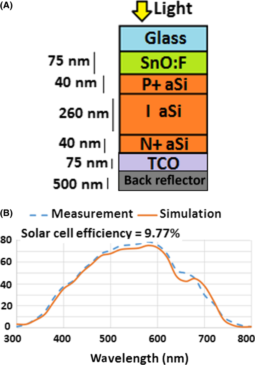
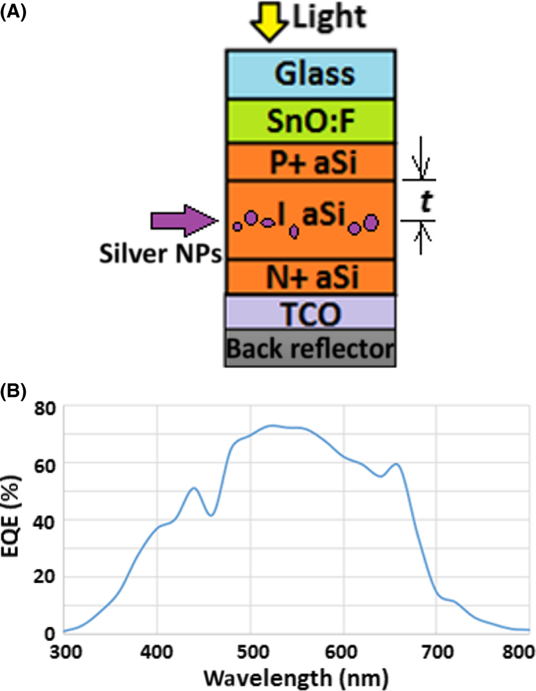
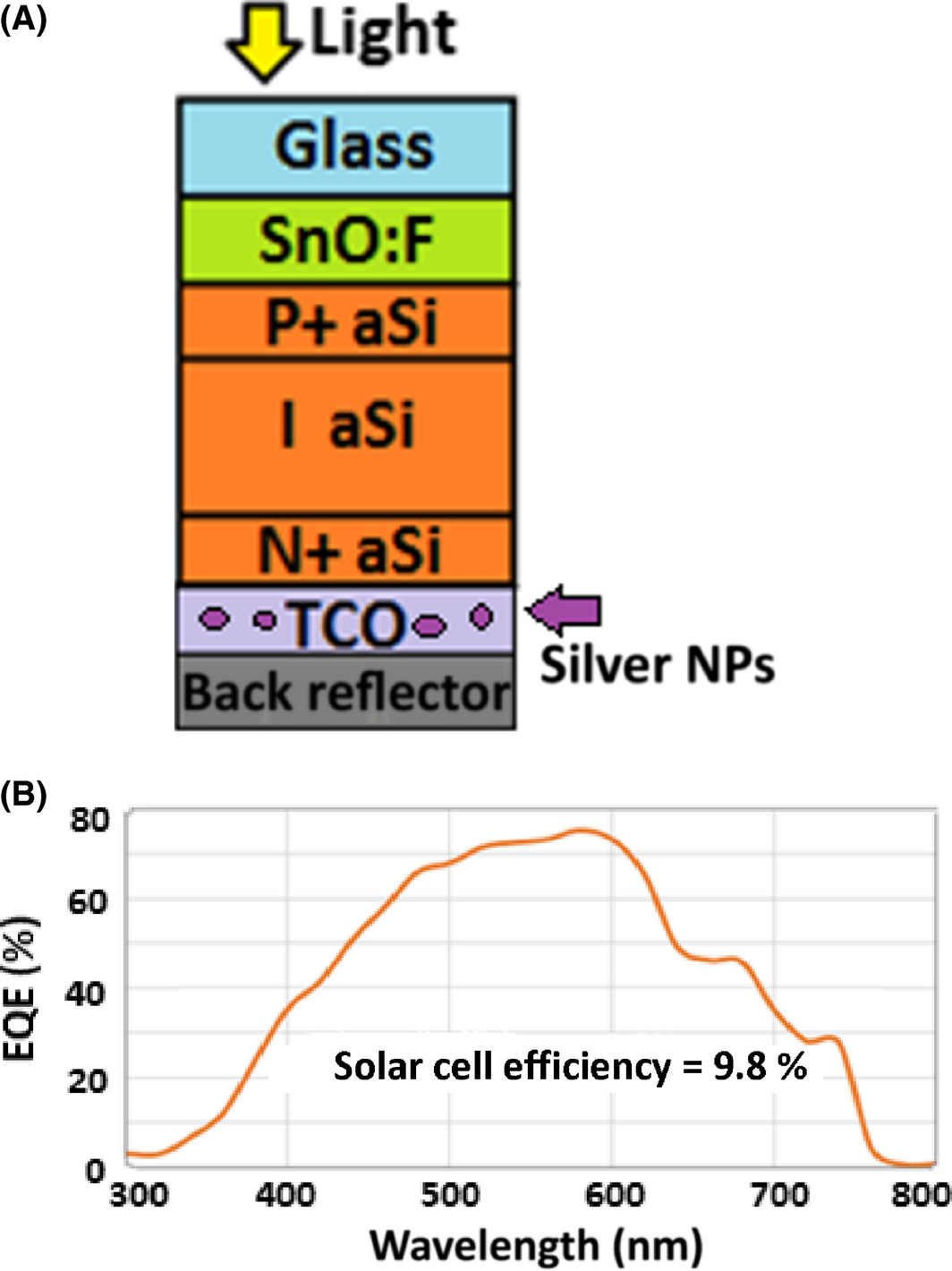
The structure of the modeled solar cell shown in Figure 1A consists of five stacked layers: a Glass (for protection) on top, a SnO:F TCO (transparent conductive oxide), followed by absorber layers (a-Si:H) as a P-I-N structure, then a TCO on the back, and all on top of a back reflector. The Amorphous silicon has 260-nm-thick intrinsic layer, the front electrode has a 75 nm-thick (SnO:F) layer, and the back electrode (AZO) is 75-nm-thick layer on top of the reflector. The N+ and P+ layers are modeled here too as 40-nm-thick layer each. Figure 1B shows a comparison between the simulated and measured EQE results, where only a slight discrepancy is seen.
|
|
|
Figure 1. (A) Schematic of the P-I-N device; (B) EQE curve (comparison between measurement [10], and simulation result). |
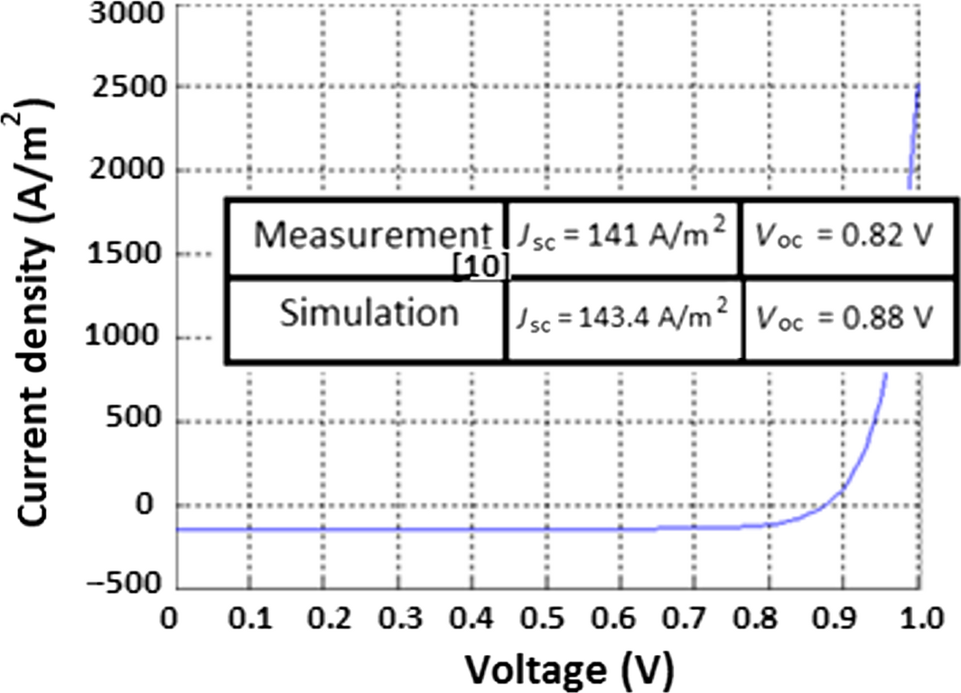
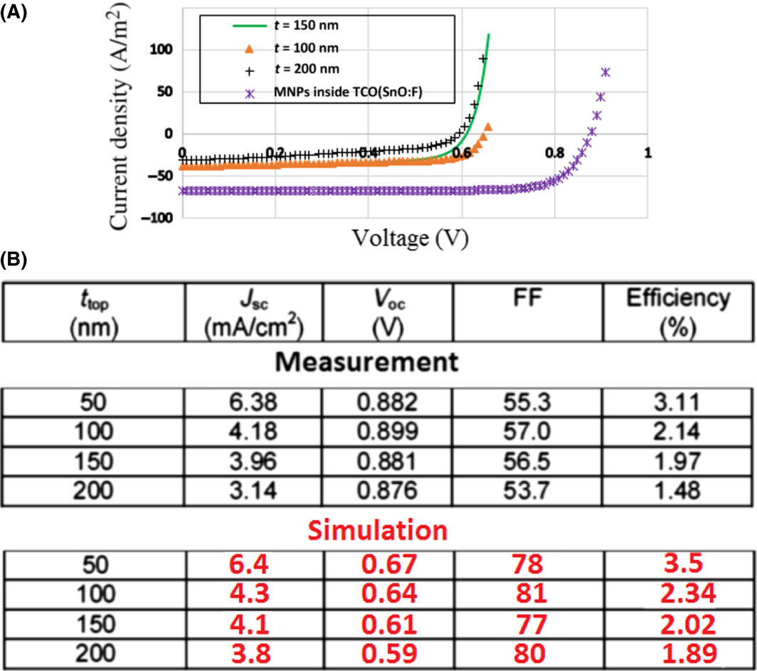
Given that most of the material parameters were obtained from well-known references (listed in Table 2) but their real values could be within a specified uncertainty range; also the physical layers dimensions were guessed based on the intended design but could deviate slightly from the fabricated ones. In addition, the dopant distribution and the density of the traps (recombination) were not listed in the experimental description and were assumed as well. Considering the approximations, the simulated results are still indicating a similar behavior to the experimentally demonstrated ones. The solar efficiency and fill factor FF were used as a base line for comparison and their values were 9.77%, and 74%, respectively, and the maximum EQE occurs at 580 nm. The calculated current density as a function of voltage is shown in Figure 2. Additionally, the measured and simulated short circuit current Jsc and the open circuit voltage Voc were listed too.
| Parameter – Name | Value |
|---|---|
| T (temperature) | 300 [K] |
| Ni -Ref [34] | 0.949 × 10⁶ [cm−3] |
| Doping (N+) | 1 × 10²⁰ [cm−3] |
| Doping (P+) | 1021 [cm−3] |
| Thickness (N+, a-Si)-Ref [10] | 40 [nm] |
| Thickness (intrinsic, a-Si)- Ref [10] | 260 [nm] |
| Thickness (P+, a-Si)- Ref [10] | 40 [nm] |
| Thickness (AZO) -(TCO in front)- Ref [10] | 75 [nm] |
| Thickness (glass)- Ref [10] | 200 [μm] |
| Thickness (Air)- Ref [10] | 20 [μm] |
| Thickness -(TCO BACK)- Ref [10] | 75 [nm](AZO) |
| Thickness (Silver) Reflector back- Ref [10] | 500 [nm] |
| Electron mobility, a-Si -intrinsic-Ref [13] | 20 [cm2/(V s)] |
| Hole mobility, a-Si -intrinsic-Ref [13] | 2 [cm2/(V s)] |
| Electron mobility, a-Si N+ -Ref [13] | 20 [cm2/(V s)] |
| Hole mobility, a-Si N+ -Ref [13] | 2 [cm2/(V s)] |
| Electron mobility, a-Si P+ -Ref [13] | 20 [cm2/(V s)] |
| Hole mobility, a-Si P+ -Ref [13] | 2 [cm2/(V s)] |
| Electron life time, a-Si -intrinsic-Ref [33, 34] | 20 [ns] |
| Hole life time, a-Si -intrinsic-Ref [33, 34] | 20 [ns] |
| Electron life time, a-Si N+ -Ref [33, 34] | 0.0001 [ns] |
| Hole life time, a-Si N+ -Ref [33, 34] | 10 [ns] |
| Electron life time, a-Si P+ -Ref [21, 22] | 10 [ns] |
| Hole life time, a-Si P+ -Ref [21, 22] | 0.0001 [ns] |
| Density of state valence band, a-Si -Ref [31] | 2.5 × 10²⁰ [cm−3] |
| Density of state conduction band, a-Si -Ref [31] | 2.5 × 10²⁰ [cm−3] |
| Difference between defect level and intrinsic level N+, P+ -Ref [27] | 0.7 |
| Difference between defect level and intrinsic level intrinsic-Ref [27] | 0.3 |
| Energy band gap a-Si-Ref [34] | 1.74 |
| Diameter silver NPs-Ref [10] | 20 [nm] |
| Affinity, a-Si (electro affinity)-Ref [13] | 4.00 eV |
| Incident light angle | 0 [deg] |
|
|
|
Figure 2. J–V curve (simulation), and a comparison between simulation and measured data [10] is shown in the embedded Table. |
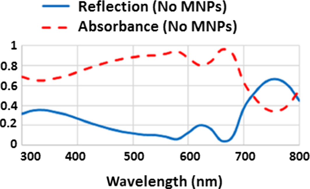
Additional parameters including the reflection and absorbance coefficient were calculated for the whole solar cell as a function of wavelength and are shown in Figure 3. The transmission coefficient, however, is almost zero.
|
|
|
Figure 3. Simulation results for solar cells without MNPs; the blue solid line represents reflection coefficient; and red dash line shows the absorbance coefficient versus wavelength. |
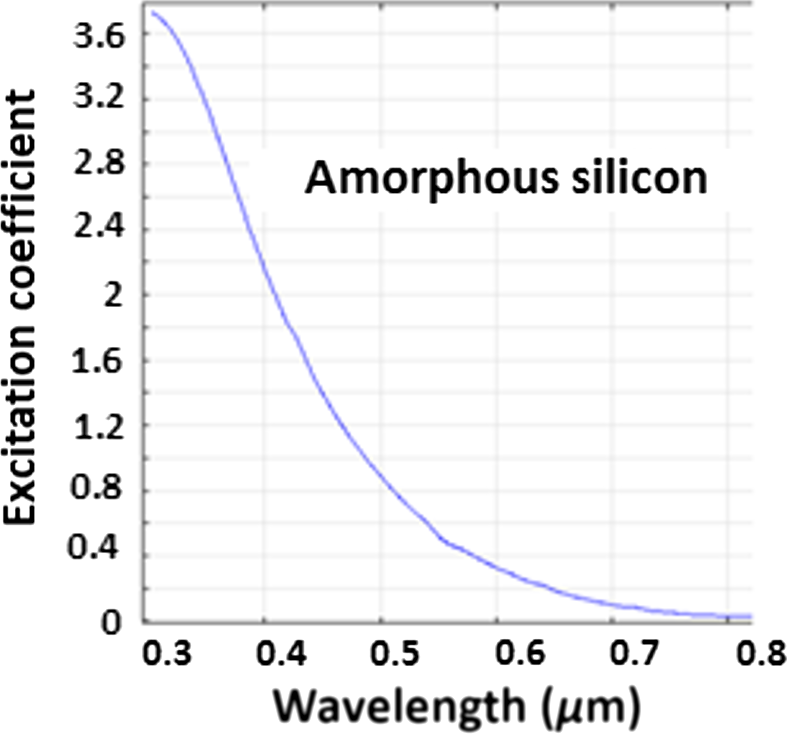
When comparing Figures 3 and 1B, the level of light absorbance coefficient in some regions of the spectrum is higher than what is indicated by the EQE curve. This difference demonstrates that the energy was not totally converted to current and this drop is due to internal device losses. Figure 4 represents the extinction coefficient of amorphous silicon calculated based on [35], and it can be observed that the absorbance of light inside the amorphous silicon increases at higher frequencies. For this reason in the UV region most of the impinging solar energy on the cell is absorbed at the top layer of the semiconductor (P+ region) before approaching the depletion region. It turns out that the probability of creating free electron-hole pairs outside the depletion region increases; thus unfortunately increasing the probability of free carrier recombination immediately and this would be an energy loss. If the light could propagate for a longer path inside the semiconductor, it can generate free electron-hole pairs inside the depletion region, subsequently the electrostatic electric field (created based on majority carriers in the depletion region) could cause charge separation (electrons and holes) creating electricity. In other words, the presence of material defects inside the semiconductors can elevate the recombination probability of free carriers as well and reduce the overall conversion efficiency.
|
|
|
Figure 4. Extinction coefficient of amorphous silicon. |
Analysis of Simulation Results of Solar Cell-no Plasmon with 3D Gratings
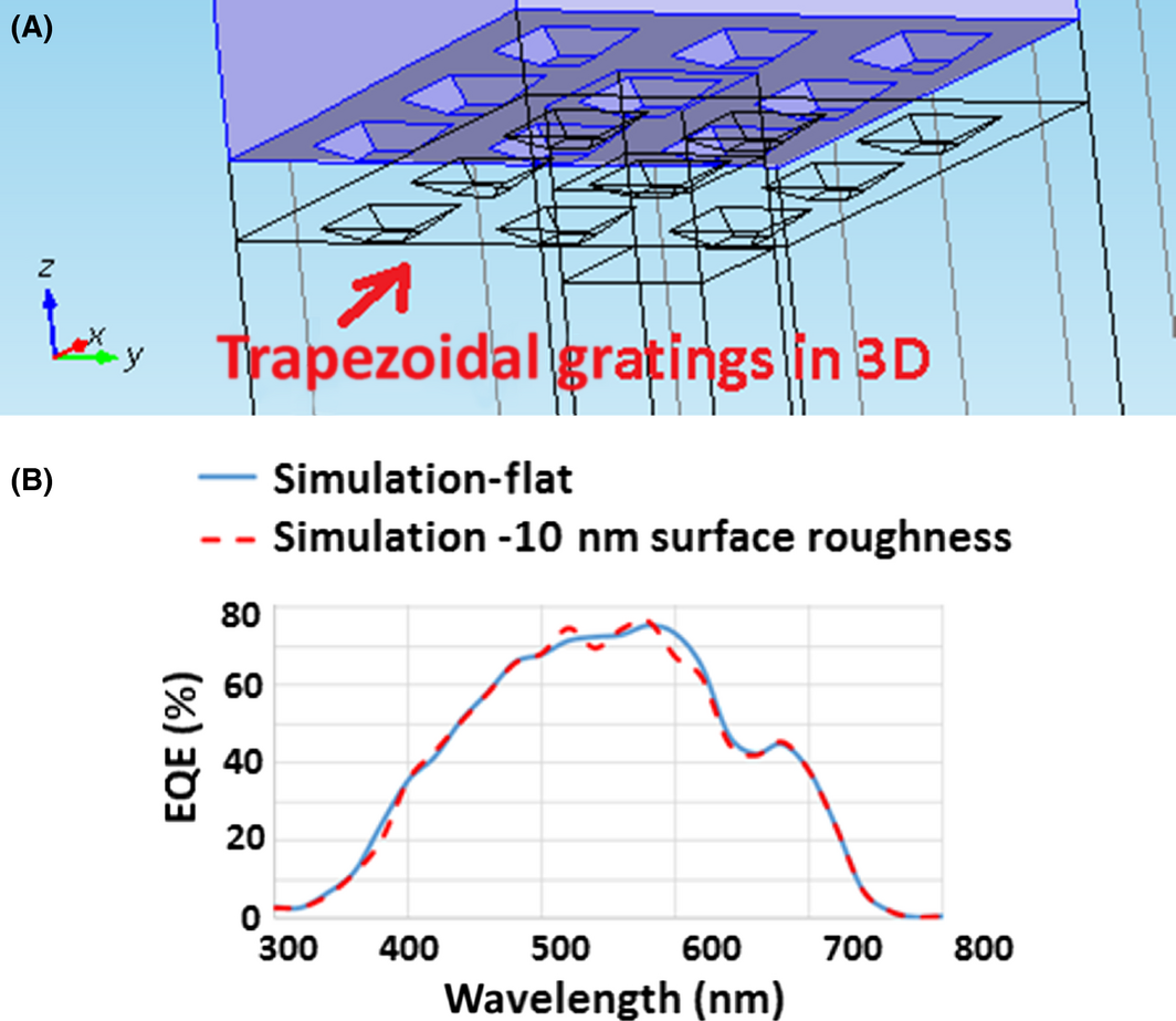
Surface roughness of solar cell layers can affect the solar cell performance. Where most of the time, the surface roughness is created by the morphology of the transparent conductive oxide (TCO) located at the top and bottom of the semiconductor layers. Use of large grains in the TCO film too can increase surface roughness [36-38]. At the same time, the size of the grains is correlated to the thickness of the thin-film TCO layer, that is, a thinner film would have less surface roughness. For instance, the thickness of the thin-film TCO considered for this model here is 75 nm, and its surface roughness is estimated to be <10 nm. To model the surface roughness effect, in general, a 3D device model can be used where a trapezoidal grating can be assumed. A periodic structure of a trapezoidal shape (like that of [17]) with a 30° degree slope in each side, and a 10 nm height (with periodicity of 200 nm) is assumed and implemented to model the 3D gratings of the solar cells (see Fig. 5A). Figure 5B shows that the results of the simulation for the EQE for both cases (flat and with gratings) are very similar for the thin-layered case. After analyzing the simulations raw data, it was clear that the surface roughness at low frequencies (IR region) is very small compared to the wavelength of solar rays. So, at these frequencies, it is a good approximation to assume that it behaves like a flat surface (from optics point of view). On the other hand, at higher frequencies (UV region) the gratings cannot be neglected, because its size is close to a wavelength. The gratings lead to ray scattering and it could cause substantial increase in light path length inside the absorber (amorphous silicon), and it is anticipated that longer path would improve solar cell efficiency. Although, no efficiency improvement has been observed in the UV region, because the absorption of the amorphous silicon in this region is very high (see Fig. 4), and the penetration depth (see Appendix A1, equations (3), (4)) is rather very small compared to the path length of the ray inside the absorber. Hence, the effect of the gratings could only be observed weakly over a narrow bandwidth (510–620 nm). Apart from slight ripples seen in Figure 5B, the assumption of a flat surface for very thin layers has been validated as the simulation results are very similar to the measurements of [10], and for simplification it will be implemented in our analysis of the effect of MNPs.
|
|
|
Figure 5. (A) schematic of the gratings in 3D inside the TCO; (B) EQE curve (comparison between simulation flat, and simulation with gratings (surface roughness = 10 nm). |
Electromagnetic Field Analysis of MNPs
One way to prove that our electromagnetic 3D model for a MNP works properly, was to validate our simulation results with an analytical method. Here, we use the well-known conic problem of scattered fields from a metallic sphere in a vacuum space (shown in Ref [39]) to validate our models for MNPs. If an electric field of a uniform plane wave is polarized in the x direction, and is traveling along the z-axis, then the monostatic radar cross section can be expressed by
|
|
(1) |
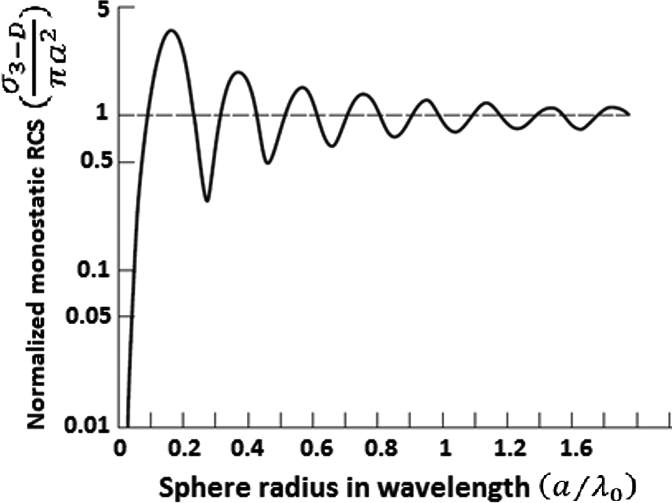
where r, Es, Ei, λ, β, a, and H(2) are represent the range, scattered electric field, incident electric field, wavelength, wave propagation constant, radius of the metallic sphere, and spherical Hankel function, respectively. A plot of equation (1) as a function of the radius of the sphere is shown in Figure 6.
|
|
|
Figure 6. Normalized monostatic radar cross section for a conducting sphere as a function of sphere radius [40]. |
The results can be divided into three regions; the Rayleigh, the Mie (or resonance), and the optical region. The Rayleigh region represents the part of the curve for small radii values (a < 0.1λ). Hence, in the Rayleigh region, equation (1) can be reduced to
|
|
(2) |
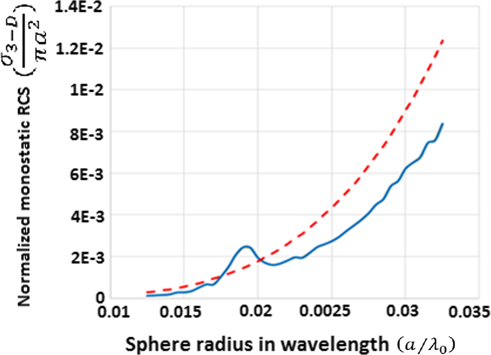
Hence, we compared our 3D model for a sphere in vacuum and the analytical method and results are shown in Figure 7. A good accuracy is seen for the long wavelengths region. Some slight deviation is, however, seen for longer wavelength but still adequate for our modeling efforts here. To improve our model at long wavelength region, finer mesh can still be used but will significantly reduce computation speed.
|
|
|
Figure 7. Normalized monostatic RCS for a single silver nanoparticle (radius = 10 nm) inside vacuum; solid blue line represents simulation result and red dash line shows the analytical method. |
Simulated and Measured Results-with Plasmon
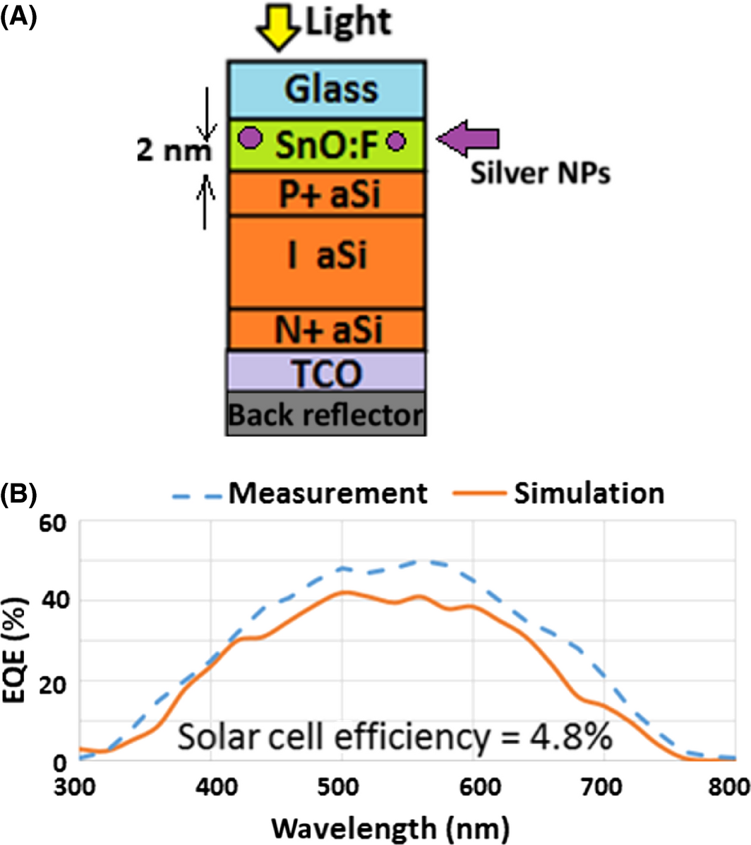
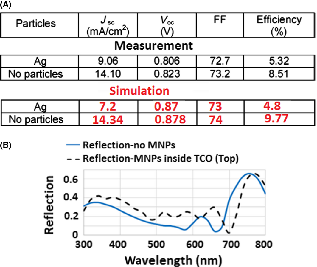
Our next step was to analyze the effect of adding silver nanoparticles in each layer; one layer at a time to determine the optimum location and position that would enhance the solar cell efficiency. In our model, silver nanoparticles are modeled as spheres with 10 nm radius [10] and are arranged in a random 2D array (in xy-plane) with a maximum center to center spacing of 50 nm. Initially, these silver NPs were placed 2 nm above the absorber layer along the SnO:F P-type A-Si interface as shown in Figure 8A as suggested by [10]. Although this resulted in a pronounced drop in solar cell efficiency as noticed in Figure 8B, which is also consistent with the observations of Ref. [10]; where the efficiency has dropped to only 4.8%. Figure 9A shows a comparison between the simulated and measured electrical outputs of a solar cell with and without MNPs. The simulated reflection coefficient for these cases are also shown in Figure 9B.
|
|
|
Figure 8. (A) Schematic of a PIN device; (B) EQE curve using MNPs embedded inside SnO:F.; blue dash line represents measurement [10]; orange solid line shows simulation. |
|
|
|
Figure 9. (A) A comparison between the measurements of [10] and simulation data for the electrical outputs; (B) Simulation results for the Reflection coefficient; solid blue line represents reflection from the solar cell without MNPs; dash black line shows reflection from the solar cell with MNPs embedded inside the TCO layer on top of the PIN device. |
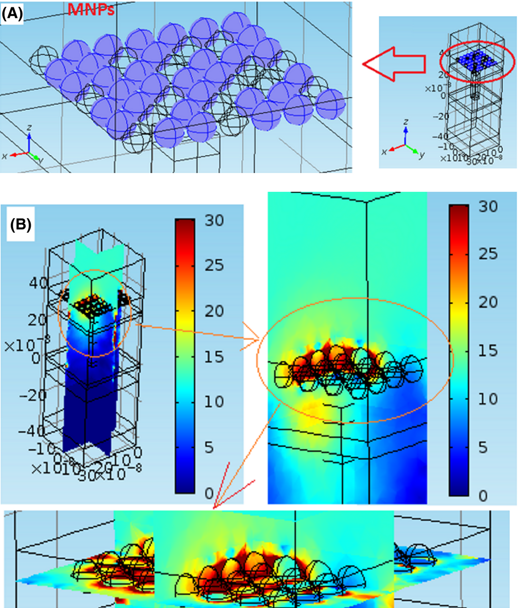
Next step, the optical behavior of the solar cell excited by a polarized plane wave is analyzed in 3D. Figure 10A shows a schematic of a random 2D array of MNPs in xy-plane. Silver nanoparticles are embedded inside TCO (on top of the PIN device). An x-polarized electromagnetic plane wave (wavelength@720 nm) is propagating in the z direction toward the structure (assuming normal incidence). The power intensity of the propagating plane wave is dropped just after passing through the MNPs (see Figure 10B). Two MNPs (next to each other) create strong localized fields (see Figure 10B) as expected.
|
|
|
Figure 10. (A) schematic of MNPs are shown as blue spheres embedded inside TCO (B) the intensity of power flow of the light (wavelength@720 nm). |
The above test was repeated, but this time with these silver nanoparticles embedded in the absorber layer (t = 50 nm under P+ layer) as seen in Figure 11A. However, it is believed that when MNPs are integrated into the amorphous silicon, they will cause an increase in the amount of defects inside the amorphous silicon structure. Unfortunately, it turns out that if this degradation phenomenon is not accounted for, then the simulation result is totally very optimistic and unrealistic. In summary, this misleading simulation result is shown in Figure 11B and indicates that significant efficiency improvement can be achieved, and as a matter of fact initially has led to a considerable confusion and a myth that adding MNPs should automatically lead to efficiency enhancement; but this has not been experimentally materialized yet due to significant fabrication defects. Practically, we needed to revise our model too to account for the impact of defects on performance, hence we modified the device physics equations as suggested by [33] to include these defects effects as well.
|
|
|
Figure 11. (A) Schematic of the PIN device; (B) EQE curve (simulation), using MNPs embedded inside intrinsic layer (t = 50 nm) without considering of defects. |
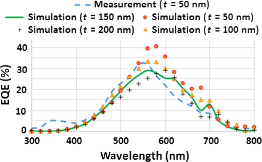
The modified model results after including the defects, gives results that are now in a fairly good agreement with measured data (Fig. 12). The results indicate a rather significant drop in efficiency which is consistent again with the observation of [10]. For t = 50 nm, the efficiency, for example, has dropped to only 3.5% in contradiction to the common belief that efficiency should have been enhanced. The pronounced efficiency drop was even worsening upon moving the MNPs from the top of the intrinsic layer to its bottom, where the solar cell efficiency dropped from 3.5% to even 1.89%. A plausible reason to explain this phenomenon is that; by varying the position of the MNPs inside the absorber and moving further down toward the bottom of the structure, the intensity of the localized field created around the MNPs decreases exponentially, because most part of the solar energy in the UV region has been absorbed significantly after passing the top layers.
|
|
|
Figure 12. EQE curve in case of existing MNPs embedded inside intrinsic layer (a-Si) blue dash line measurement (t = 50 nm) [10]; other curves represents simulation results (after considering of defects). |
Hence, fields would become very weak to excite the MNPs. For this reason the generation rate compared to the recombination rate in the intrinsic layer goes down upon moving the MNPs toward the bottom. The simulation result for the JV curves, with existing MNPs in different locations inside the solar cells are shown in Figure 13A. Figure 13B shows the electrical outputs for the measured [10] and simulated data. Finally, the silver NPs were relocated to the back (embedded inside the TCO), and that represented the most suitable location as seen in Figure 14A. The maximum solar efficiency now is 9.8% which is very close to the solar cell case with no NPs (see Fig. 14B). Again this observation is consistent with [10], but definitely much lower than our expectation of enhancing the efficiency upon adding MNPs.
|
|
|
Figure 13. (A) J–V curve of the solar cell; for existing MNPs inside the structure; (B) comparison electrical outputs from measurement [9], and simulation. |
|
|
|
Figure 14. (A) Schematic of the PIN device; (B) EQE curve (simulation), using MNPs embedded inside TCO (back). |
Conclusion
In this study, an effective rigorous 3D multiphysics modeling of solar cells was presented. Our developed simulator is a real multiphysics modeling toolbox that is comprised of three coupled modules: Optics, carrier transport in semiconductors, and Electrostatic. To solve their associated nonlinear partial differential equations (PDEs) in 3D, we used two commercial tools (COMSOL, and MATLAB). One of the main reasons to carry out this 3D simulation is to accurately predict the electric field distribution due to the light scattering of the 3D plasmonic particles excited by the randomly polarized sun light. Our 3D tool has been validated by comparing its results with published measured ones.
The comparison between both measured and simulated results indicates a very good agreement even though some material parameters were assumed like the dopant distribution, and the density of traps (recombination), in addition to some assumed layers' thicknesses. The developed toolbox has been used to observe some major phenomena like strong localized fields around the MNPs and relate intense recombination to defects. The presence of MNPs might be helpful to enhance light absorption, although it would not guarantee improving solar cells' efficiency. Our simulation results demonstrated too that the trap density caused by defects around MNPs is the main reason for efficiency degradation that was seen experimentally. Here, we have verified that embedding MNPs randomly can lead to a significant external quantum efficiency degradation which is consistent with various experimental observations. Meanwhile, relocating the MNPs to the TCO layer close to the bottom electrode could provide some efficiency enhancement even though not pronounced. So, work is still under way to simulate other cases using our 3D toolbox to get significant efficiency improvement and to address the defect degradation issue, preliminary results are encouraging but would require more validation at this point.
Acknowledgments
This work was supported by the grant from the National Science Foundation of USA (Grant No. NSF EPS-1004083).
Conflict of Interest
None declared.
Appendix A1: Solving Solar Cell Problem in 3D
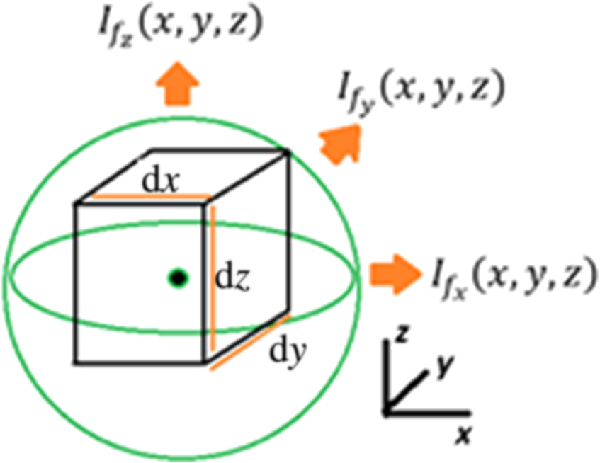
If α and If(x, y, z) are the absorption coefficient and the intensity of the photons at position (x, y, z), respectively (Fig. 15), then the relationship for the optical absorption for the differential length (Dx, Dy, Dz) is given bellow.
|
|
|
Figure 15. Photon intensity in a 3D cell. |
|
|
(3) |
|
|
(4) |
This equation clearly shows that the intensity of a photon decreases exponentially with the propagation distance through the semiconductor material due to the absorption [25, 27-29]. Meanwhile, the number of electron-hole pairs generated by the light is:
Generation rate [28]:
|
|
(5) |
where h is plank constant, and f is frequency of the wave.
Subsequently, to calculate the free electron density and free hole density, Poissons Equation is used:
|
|
(6) |
Shockley Read Hall recombination rate ((7)-(11)) [42, 43]:
|
|
(7) |
|
|
(8) |
|
|
(9) |
|
|
(10) |
|
|
(11) |
|
|
(12) |
Transport of Diluted species (Electron)
|
|
|
|
(13) |
|
|
|
|
(14) |
|
|
(15) |
where ϕ (Electric Potential), p (Hole concentration), and n (Electron concentration) are variables, q (Electron charge), ε (Optical property of the material), c (Initial value for carrier concentration), ni (intrinsic concentration), τn (Electron life time), τp (Hole life time), φ0 (incident photon flux), α, (absorption coefficient of material), μn (Electron mobility), μp (Hole mobility), and Dn (Electron Diffusivity) are constants.
γn and γp are the electron and hole degeneracy factors, Nc and Nv are the effective densities of states for the conduction and valence band, Eg is the band gap, ∆Eg the band gap narrowing and Et is the trap energy level. Energy difference between the defect level and the intrinsic level is ∆Et.
The same equations can be derived for holes.
After coupling equations (13), (14), and (15), there will be only two nonlinear PDEs (16), (17).
|
|
(16) |
|
|
(17) |
Gaussian distribution (for both acceptor and donor) is considered as a dopant distribution. The junction depths in x, y, and z direction are set at 2 μm, 2 μm, and 300 [nm], respectively.
Figure A1 is shown in below that could be a good representation of our 3D model.
|
|
|
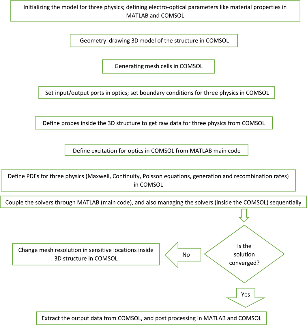
Figure A1. The flow diagram of the 3D model. |
The flowchart clearly shows that the proposed solution is a staggered one, and not a fully coupled one. First, the optical problem is solved. Then the two other physics (the semiconductor device and the electrostatic) are solved sequentially.
In this analysis, the PDEs are solved in steady state. So the transient solutions are not considered. It means that . The excess minority carrier hole concentration increases with time with the time constant (which is the excess minority carrier lifetime). The excess carrier concentration reaches a steady-state value as time goes to infinity, even though a steady-state generation of excess electrons and hole exists [28]. The generation rate G a function of wavelength and time. However, here we are solving only for steady state and ignore any time dependence. Wavelength dependence is often included by summing the result obtained at one wavelength over all wavelengths of interest.
The RF interfaces formulate and solve the differential form of Maxwells equations together with the initial and boundary conditions. The equations are solved using the finite element method. The steps are defined from MATLAB, and it can control COMSOL through a live link.
1-Define the geometry 2-Select materials 3-Select a suitable RF interface 4-Define boundary and initial conditions 5-Define finite element mesh 6-Define PDEs 7-Visualize the results.
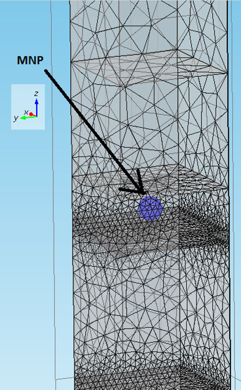
To minimize the amount of physical memory (RAM) for computation and speed up computation we can use periodic boundary conditions along x, and y axis, which means that we solve equations for only one unit cell. Tetrahedral has been chosen as a type of mesh. Sharp edges or small particles like MNPs should be generated with high mesh density. Also the mesh size physically placed close to the critical edges (p and n type region) should be considered fine to make sure the PDEs solver is converged properly (Fig. 16).
|
|
|
Figure 16. Tetrahedral Mesh Generation of the 3D device for one unit cell. |
Appendix A2: Initialization of the Simulator
In order to solve these partial differential equations, all parameters are needed to be initialized. The electro-optical properties like dielectric constant, refractive indices (real part and imaginary part), electron/hole mobility and the other electronic properties have been extracted from [13], [30-34]. In case of using MNPs or a plasmon layer the dielectric constant value has to be calculated for each optical wavelength of interest. For gold or silver NPs, optical constants were measured and given by Drude [44]. Drude-Lorentz dispersion model is a well-known model and is given by
|
|
(18) |
Additional references can be used like [45, 46] to double check materials properties.
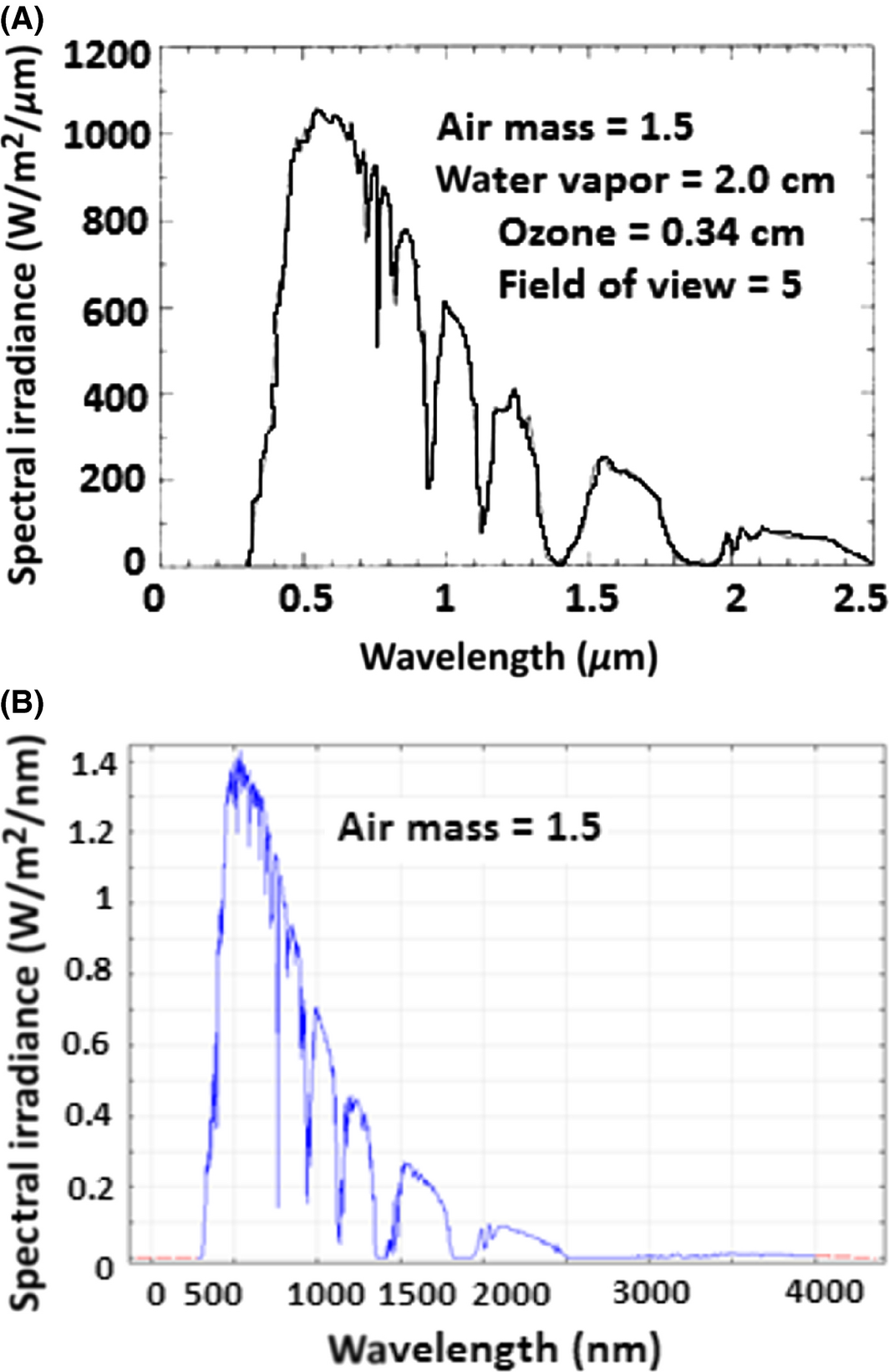
Generally, the spectrum of incident light and intensity of impinging on the device is the most important initializing step to get accurate results from the simulation. Because some of the simulation outputs (like solar cell efficiency, and short circuit current) are directly related to the impinging light intensity as a function of wavelength, we needed then to utilize very accurate data. Hence, we utilized the spectral irradiance chart that has been measured several times and published by NASA [41] (Fig. 17A). Although, we need to keep in mind that the spectral irradiance depends on different factors like: the height from the sea level, water vapor, and air pollution. It is time dependent as well. For simplicity, we assume as a constant for the time being. Figure 17B shows the latest update that was found from [26], and utilized in our simulator.
|
|
|
Figure 17. (A) Standard solar spectrum generated with the BRITE Monte Carlo Solar Insolation Model using the atmospheric conditions specified in [41]; (B) the utilized update of the spectral irradiance—downloaded from [26]. |
Appendix A3: Electrical Outputs
Our model can be used to calculate many parameters like: External Quantum Efficiency (EQE), Solar Cell Efficiency, open circuit voltage, and short circuit [27, 28].
The external quantum efficiency (EQE) is defined as:
|
|
(19) |
The short-circuit current density can be computed as:
|
|
(20) |
|
|
(21) |
FF is the filling factor, which can be derived from J–V curve of the device.
|
|
(22) |
References
- Zeman, M.2006. Advanced amorphous silicon solar cell technology. Pp. 173–236inJ. Poortmans, V. Archipov, eds. Thin film solar cells: fabrication, characterization and applications. Wiley, Chichester. ISBN: 978-0-470-09126-5.
- Deckman, H. W., C. B. Roxlo, and E. Yablonovitch. 1983. Maximum statisticalincrease of optical absorption in textured semiconductor films. Opt. Lett.8:491–493.
- Isabella, O., F. Moll, J. Krcˇ, and M. Zeman. 2010. Modulated surface textures using zinc-oxide films for solar cells application. Phys. Status Solidi A207:642–646.
- Kambe, M., A. Takahashi, N. Taneda, K. Masumo, T. Oyama, and K. Sato. 2008. Fabrication of a-Si:H solar cells on high haze SnO2:F thin films. p. 1, in Photovoltaic Specialist Conference, San Diego, USA. 33rd IEEE (doi: 10.1109/PVSC.2008.4922507)
- Borri, C., and M. Paggi. 2015. Topological characterization of antireflective and hydrophobic rough surfaces: are random process theory and fractal modeling applicable?J. Phys. D: Appl. Phys.48:045301.
- Haug, F.-J., T. Söderström, O. Cubero, V. Terrazzoni-Daudrix, X. Niquille, S. Perregeaux, et al. 2008. Periodic textures for enhanced current in thin film silicon solar cells. Mater. Res. Soc. Symp. Proc.1101:KK13–KK. doi: 10.1557/PROC-1101-KK13-01.
- Zeman, M., O. Isabella, K. Jäger, R. Santbergen, S. Solntsev, M. Topic, and J. Krc. 2012. Advanced Light management approaches for thin-film silicon solar cells. Energy Procedia15:189–199.
- Pahud, C., O. Isabella, A. Naqavi, F.-J. Haug, M. Zeman, H. P. Herzig, et al. 2013. Plasmonic silicon solar cells: impact of material quality and geometry. Opt. Express21:A786–A797. doi: 10.1364/OE.21.00A786.
- Toroghi, S., L. Chatdanai, and P. G. Kik. 2013. Cascaded plasmon resonances multi-material nanoparticle trimers for extreme field enhancement. Proc. SPIE 8809, Plasmonics: Metallic Nanostructures and Their Optical Properties XI, 88091M. doi: 10.1117/12.2024709.
- Santbergen, R., A. H. M. Smets, and M. Zeman. 2011. Silver nanoparticles for plasmonic light trapping in A-Si:H solar cells. Pp 000673–000678in Photovoltaic Specialists Conference (PVSC), 37th IEEE, Seattle, WA.
- Stuart, H. R., and D. G. Hall. 1998. Island size effects in nanoparticle-enhanced photodetectors. Appl. Phys. Lett.73:3815.
- Malm, U., and M. Edoff. 2009. 2D device modelling and finite element simulations for thin-film solar cells. Sol. Energy Mater. Sol. Cells93:1066–1069.
- Ihalane, E., M. Meddah, A. Elfanaoui, L. Boulkaddat, E. El Hamri, X. Portier, et al. 2011. Numerical simulation of photocurrent in a solar cell based amorphous silicon. Moroccan J. Condens. Matter. 13:83–87.
- Basore, P. A.1990. Numerical modeling of textured silicon solar cells using PC-1D. IEEE Trans. Electron Devices37:337–343.
- Degrave, S., M. Burgelman, and P. Nolle. Modelling of polycrystalline thin film solar cells: new features in scaps version 2.3. 3rd World Conference on Pholovolroic Lnirergv Conversion Mov 11–18, 2003 Osaka, Japan.
- Barrera, M., F. Rubinelli, I. Rey-Stolle, and J. Pla. 2012. Numerical simulation of Gesolar cells using D-AMPS-1Dcode. Phys. B407:3282–3284.
- Isabella, O., S. Solntsev, and M. Zeman. 2013. 3-D optical modeling of thin-film silicon solar cells on diffraction gratings. Prog. Photovoltaics Res. Appl.21:94108.
- Li, X., N. P. Hylton, V. Giannini, K.-H. Lee, N. J. Ekins Daukes, and S. A. Maier. 2011. Bridging electromagnetic and carrier transport calculations for three-dimensional modelling of plasmonic solar cells. Opt. Express19:A888–A896.
- Deceglie, M. G., V. E. Ferry, A. P. Alivisatos, and H. A. Atwater. 2012. Design of nanostructured solar cells using coupled optical and electrical modeling. Nano Lett.12:2894–2900. doi: 10.1021/nl300483y.
- Yee, K. S.1966. Numerical solution of initial boundary value problems involving Maxwells equations. IEEE Trans. Antennas Propag.14:302–307.
- Weiland, T.1977. A discretization method for the solution of Maxwells equations for six-component fields. Int. J. Electron. Commun. AEU31:116–120.
- Moharam, M. G., and T. K. Gaylord. 1981. Rigorous coupled-wave analysis of planar-grating diffraction. J. Opt. Soc. Am.71:811–818.
- Gibson, W. C.2008. The method of moments in electromagnetics. Chapman & Hall/CRC, Boca Raton. ISBN 978-1-4200-6145-1.
- Jin, J.-M.2002. The finite element method in electromagnetics, 2nd ed. John Wiley & Sons, New York. ISBN 978-0-471-43818-2.
- Quinn, J. J., and K.-S. Yi. 2009. Solid state physics: principles and modern applications. Springer-Verlag, Berlin Heidelberg.
- Dewan, R., S. Fischer, V. B. Meyer-Rochow, Y. Özdemir, S. Hamraz, and D. Knipp. 2012. Studying nanostructured nipple arrays of moth eye facets helps to design better thin film solar cells. Bioinspir. Biomim.7:016003.
- SZE. 1981. Physics of semiconductor devices, 2nd ed. Wiley-Interscience, New York.
- Neamen, D. A.2003. Semiconductor physics and devices: basic principles, 3rd ed.McGraw Hill, New York.
- Madelung, O.2004. Semiconductors: data handbook. Springer-Verlag Berlin Heidelberg.
- Deng, X., and E. A. Schiff. 2005. Amorphous silicon–based solar cells, chapter 12. John Wiley & Sons, Ltd, Chichester, UK.
- Bakr, N. A., A. M. Funde, V. S. Waman, M. M. Kamble, R. R. Hawaldar, D. P. Amalnerkar, et al. 2010. Determination of the optical parameters of a-Si:H thin films deposited by hot wire–chemical vapor deposition technique using transmission spectrum only. Pramana J Physics.76:519–531.
- Alamo, J. A., and R. M. Swanson. 1987. Modeling of minority-carrier transport in heavily doped silicon emitters. Solid-State Electron.30:1127–1136.
- Piprek, J.2003. Semiconductor optoelectronic devices introduction to physics and simulation. Academic Press; 1 edition (January 21, 2003). ISBN-13: 978-0125571906.
- Sakata, I., and Y. Hayashi. 1985. Theoretical analysis of trapping and recombination of photo generated carriers in amorphous silicon solar cells. Appl. Phys. A37:153–164.
- Pierce, D. T., and W. E. Spicer. 1972. Electronic structure of amorphous SI from photoemission and optical studies. Pierce Spicer Phys. Rev. B.5:3017.
- Gracia, M., F. Rojas, and G. Gordillo. Morphological and optical characterization of SnO2:F thin films deposited by spray pyrolysis. 20th European Photovoltaic Solar Energy Conference, 6–10 June 2005, Barcelona, Spain.
- Chaaya, A. A., R. Viter, M. Bechelany, Z. Alute, D. Erts, A. Zalesskaya, et al. 2013. Evolution of microstructure and related optical properties of ZnO grown by atomic layer deposition. Beilstein J. Nanotechnol.4:690–698. doi: 10.3762/bjnano.4.78.
- Kumar, V., N. Singh, R. M. Mehra, A. Kapoor, L. P. Purohit, and H. C. Swart. 2013. Role of film thickness on the properties of ZnO thin films grown by sol-gel method. ELSEVIER Thin Solid Films539:161–165.
- Balanis, C. A.1989. Advanced engineering electromagnetics. Wiley, Hoboken, New Jersey, USA.
- Aden, A. L.1951. Scattering from spheres with sizes comparable to the wavelength. J. Appl. Phys.22:601.
- http://www.astm.org/Standards/G159.htm.
- Hall, R. N.1952. Electron-hole recombination in silicon. Phys. Rev.87:387.
- Shockley, W., and W. T. Read. 1952. Statistics of the recombinations of electrons and holes. Phys. Rev.87:835–842.
- Johnson, P. B., and R. W. Christy. 1963. Optical constants of the noble metals. Phys. Rev. Lett.11:541.
- OptiFDTD: Technical Background and Tutorials.
- Terrestrial photovoltaics measurement procedures, NASA Tech. Memo. TM 73702, National Aeronautics and Space Administration, Cleveland, OH, 1977.
Document information
Published on 01/06/17
Submitted on 01/06/17
Licence: Other
Share this document
Keywords
claim authorship
Are you one of the authors of this document?
