Abstract
Three different multiple-valued logic (MVL) designs using the multiple-peak negative-differential-resistance (NDR) circuits are investigated. The basic NDR element, which is made of several Si-based metal-oxide-semiconductor field-effect-transistor (MOS) and SiGe-based heterojunction-bipolar-transistor (HBT) devices, can be implemented by using a standard BiCMOS process. These MVL circuits are designed based on the triggering-pulse control, saw-tooth input signal, and peak-control methods, respectively. However, there are some transient states existing between the multiple stable levels for the first two methods. These states might affect the circuit function in practical application. As a result, our proposed peak-control method for the MVL design can be used to overcome these transient states.
Keywords
Multiple-valued logic ; Negative differential resistance circuit ; BiCMOS process ; Peak-control method
1. Introduction
Multiple-valued logic (MVL) circuits offer several potential applications for the improvement of modern circuit designs. The origin of MVL was from the Lukasiewicz logic idea [1] . The MVL can transfer more information with fewer interconnects between devices as compared to traditional binary logic. We can use the MVL domain for more efficient solution of binary problem, thus achieving high-speed arithmetic operations. It can also provide more compact solutions and better functional capabilities in the information process [2] and [3] .
MVL circuits could be implemented in bipolar technology such as integrated injection logic (I2 L) [4] and emitter-coupled logic (ECL) [5] . Because the silicon gate MOS transistor replaced bipolar circuits as the main device in circuit design, there were some reports that used the MOS or CMOS technology to design the MVL circuits [6] , [7] , [8] , [9] and [10] . There were two main technologies such as current mode [11] and voltage mode [12] , which could be used to design the MOS-based MVL circuits. Recently, the carbon nanotube was used to design the MVL circuits [13] and [14] . Among these technologies, there are two potential candidates for commercial purposes, which are current-mode CMOS technology and negative-differential-resistance devices [15] .
The negative differential resistance (NDR) device has remarkable property due to its folded current–voltage (I–V) curve. The well-known NDR devices are Esaki diode and resonant-tunneling diode (RTD). Their NDR characteristics can provide very attractive and useful ideas for some applications [16] , [17] and [18] . In particular, the multiple-peak NDR circuits provide the convenience to design the MVL circuits. Several MVL circuits were demonstrated by using the RTD [19] and [20] , the resonant interband tunneling diode (RITD) [21] , and quantum dot gate FETs [22] .
The RTD made by III–V materials including GaAs and InP is not compatible with the mainstream ULSI technology, such as the CMOS or BiCMOS process. The fabrication of the RTD-based applications involves the use of the molecular-beam-epitaxy (MBE) or metal-organic-chemical-vapor-deposition (MOCVD) system. If the RTD-based applications need to integrate with the Si-based active and passive devices to achieve the system on a chip, the process for the integration of the MOCVD system with the CMOS technique is not easy. This limits the development of the RTD-based applications. Therefore, if we can fabricate the NDR-based circuits using the CMOS or BiCMOS technique, it is very attractive in the commercial applications. Besides, the circuit can be simulated using the HSPICE program, which is the most popular CAD tool in the IC design.
In recent years, there were some reports on Si-based RITD structures [23] and [24] , and some of them were successfully integrated with the Si-based CMOS [25] and the SiGe heterojunction-bipolar-transistor (HBT) [26] , making these devices promising for future applications. However, they still need the MBE system to accomplish the combined circuits and applications. In this work, we propose a MOS-HBT-NDR NDR circuit, which is made of several standard Si-based MOS devices and SiGe-based HBT devices. A four-valued logic circuit is demonstrated using a three-peak NDR curve that is made of three series-connected MOS-HBT-NDR circuits.
A traditional NDR-based MVL circuit requires a load device to bias the multiple-peak NDR circuit to obtain the stable logic states. We present three different MVL designs by using a resistor as a load, because it is a simple and direct method. However, the first two circuits showed that some transient states existed in the output results. Those transient states were located between the stable states. The states were so high that they might result in error transfer in the information system. To overcome this problem, we designed the third MVL circuit using the voltage-controlled MOS-HBT-NDR circuit, where the peaks of the multiple-peak I–V characteristics could be controlled by the external voltages. Using this method, we designed a voltage-controlled MVL circuit with four clear logic states, and there was no transient state occurring between two stable states. This NDR-based MVL circuit was designed according to the standard SiGe BiCMOS process provided by the Taiwan Semiconductor Manufacturing Company (TSMC) foundry.
2. Basic NDR and MVL circuit design
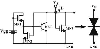
The MOS-HBT-NDR circuit used in this work is made of three Si-based n-channel MOS and one SiGe-based HBT devices, as shown in Fig. 1 . The circuit can show the NDR I–V characteristic by determining the appropriate gate width/length (W/L) parameters of the MOS devices. In view of the operation of this MOS-HBT-NDR circuit, we should apply a fixed voltage Vgg and increase the bias VS gradually. The magnitude of the Vgg must be larger than the sum of threshold voltage of the MN1 device and the turn-on voltage of the HBT device. The MN1 device is connected like a diode and is always turned on during circuit operation. The MN2 device is operated as a variable resistor as we increase the bias VS gradually. The combined current is the sum of the collector current of the HBT device and the drain current of the MN3 device. Because the MN1 and MN2 devices can be regarded as a voltage divider, the node voltage between them can be used to control the operation situation of the HBT device.
|
|
|
Fig. 1. Circuit configuration of a MOS-HBT-NDR circuit. |
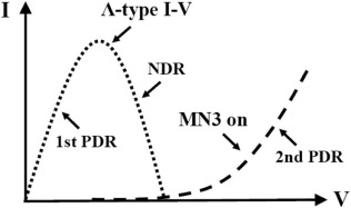
When we apply a small voltage VS , the operation of the MN1 device is saturated and the MN2 device is turned off. The current is proportional to this voltage. This region is the first positive-differential-resistance (PDR) segment of the combined I–V curve. If we further increase the bias VS , the MN2 device is turned on and the base voltage of the HBT device is decreased gradually. It results in the decrease of the collector current gradually. This region is the NDR segment of the combined I–V curve. Finally, the bias VS is high enough to make both the MN1 and MN2 devices saturated. When the node voltage between the MN1 and the MN2 devices is smaller than the turn-on voltage of the HBT device, the HBT device is turned off. Therefore, the combined current of the MN1, MN2, and HBT devices is presented as a Λ-type I–V characteristic, as the dotted lines shown in Fig. 2 .
|
|
|
Fig. 2. I–V characteristic of a MOS-HBT-NDR circuit. |
The MN3 device is connected like a diode and controlled by the bias VS . When the bias VS is larger than the threshold voltage, its I–V characteristic is an exponential curve, as the broken lines shown in Fig. 2 . This establishes the second PDR segment of the combined I–V characteristic. Finally, we can obtain an N-type I–V curve in the combined NDR circuit by increasing the bias VS gradually. Notice that the NMOS of the MN1 and MN3 devices can be replaced by the PMOS devices. The HBT device can be replaced by the BJT or NMOS device. Therefore, this NDR circuit can be implemented by using the CMOS or BiCMOS technique.
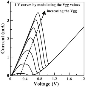
In particular, this NDR circuit possesses the ability to control the peak current by the external voltage terminal Vgg. If we increase the voltage Vgg, the base voltage of the HBT device is increased too. This results in the increase of the collector current of the HBT device. Therefore, we can obtain higher peak current. Fig. 3 shows the simulated I–V characteristics by varying the Vgg values from 1.5 V to 2.7 V with a step of 0.2 V. The MOS parameters were designed as WMN1 = 3 µm, WMN2 = 10 µm, WMN3 = 10 µm and LMN1,2,3 = 0.35 µm. The HBT was used the standard ln02 cell based on the standard 0.35 µm SiGe process provided by the TSMC foundry. When the Vgg is biased at 2.1 V, the simulated peak voltage is 0.55 V, valley voltage is 0.85 V, peak current is 2 mA, and valley current is 0.25 mA. The peak-to-valley current ratio (PVCR) is about 8.
|
|
|
Fig. 3. I–V characteristics of a MOS-HBT-NDR circuit by modulating the Vgg values. |
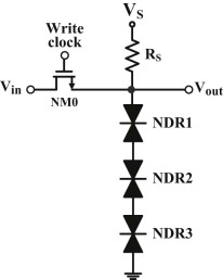
When N NDR devices are integrated vertically, we can obtain N peaks, N valleys, and N + 1 PDR segments in the combined I–V characteristics. Using the N + 1 PDR segments, we can design a (N + 1)-valued logic circuit [27] . Therefore, we can design a four-valued logic circuit based on a three-peak NDR curve. Fig. 4 shows the circuit configuration of our proposed MVL circuit, which is consisted of three series-connected MOS-HBT-NDR circuits, which are named as NDR1, NDR2, and NDR3. This MVL circuit is biased by a suitable voltage source VS through a load resistor RS .
|
|
|
Fig. 4. Configuration of a MOS-HBT-NDR-based MVL circuit. |
The combined current is strongly dependent on the parameters of the devices. The turning on sequence of such series-connected NDR circuit follows a simple rule; that is, the NDR circuit with the smallest peak current is always turned on first. Therefore, the peak currents of the three-peak NDR I–V characteristics are shown from the smallest to the largest in sequence. The gate widths were designed as WMN1 = 3 µm, WMN2 = 40 µm, and WMN3 = 40 µm for three NDR circuits. The HBT device uses the standard ln02 cell. The gate lengths were fixed at 0.35 µm.
We implemented this three-peak NDR circuit using the standard 0.35-µm SiGe BiCMOS process provided by the TSMC foundry. This IC layout must pass a series of checks including the layout versus schematic, design rule checking, and parasitic extraction before the tapeout. We also needed to consider the effect of environmental differences on the circuit function such as the bias deviation with ±10% and the operating temperature under −25 °C, 0 °C, 40 °C, and 70 °C, respectively. We could obtain the result under a reasonable range. We also need to consider the layout optimization of interconnection [28] . The cell area of this chip was occupied about 50 × 100 µm2 . The area can be improved by redesigning the MOS parameters using a scale-down process. There were only twelve transistors used in this MVL circuit. The number of devices and the chip area were greatly reduced in comparison with the CMOS-based MVL circuit discussed in Reference [6] .
The BiCMOS process has many advantages over the CMOS technique, such as higher switching speed, better noise performance, and better high-frequency characteristics. In addition, the BiCMOS process follows almost the same scaling curve as the CMOS technology, which may lead to significant effects in the BiCMOS products in the future.
3. MVL measured results
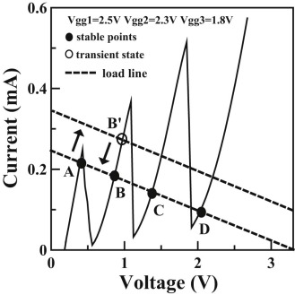
According to our simulation results, the peak currents can be revised by inputting different Vgg values. Here, the Vgg values are set at Vgg1 = 2.5 V, Vgg2 = 2.3 V, and Vgg3 = 1.8 V, respectively. The measured I–V curve is shown in Fig. 5 . There are three peaks, three NDR regions, and four PDR segments. The magnitudes of the three peak currents are shown as IP1 < IP2 < IP3 . The PVCR is one of the figure-of-merits for the evaluation of the I–V performance of a NDR circuit. Here we obtain IP1 = 0.26 mA, IV1 = 0.01 mA, IP2 = 0.37 mA, IV2 = 0.03 mA, IP3 = 0.52 mA, and IV3 = 0.05 mA. Therefore, the PVCR values are 26, 12.3, and 10.4 for three peaks, respectively. These values are higher than those shown in the multiple-peak RTD and RITD circuits [19] , [20] and [29] . For the MVL application, the optimization of the PVCR of each peak should be larger than 10. If we input a higher Vgg value, we can obtain a higher peak current. The high and adjustable PVCR characteristics are the benefits in designing the MVL circuit.
|
|
|
Fig. 5. I–V characteristic and load-line analysis for a four-valued logic circuit. |
There are two traditional methods to bias this three-peak NDR circuit. One method is to use a constant current source as the load. This kind of MVL circuit possesses a better noise margin because the load current is adjusted to a value approximately halfway between the peak and the valley currents. After designing a constant current source, we should suitably arrange the input signal along with the write circuit.
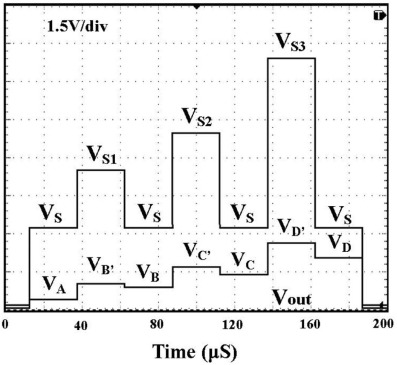
Another method is to use a resistor as a load device. This approach is a direct and easy design. Because we focus on making a comparison between three different MVL structures, a resistor is used in this work. The resistance is estimated to be 13.5 KΩ here. The load line intersects the PDR segments with four operating points from A to D in order, as shown in Fig. 5 . The voltage to be stored can be provided by enabling the VS as a pulse signal. First, the operating point is located at point A. The stable logic state is VA . We can input a positive triggering pulse to transfer the logic state from operating points A to B, as shown by the top-right arrow direction. The rising triggering pulse intersects the second PDR segment at point B′. When the falling triggering pulse returns to the load-line base, as shown by the lower-left arrow direction, the operating point is located at point B. At this moment, we can obtain the transfer of logic state from VA to VB . The voltage level corresponding to the triggering pulse is called the transient state here. Therefore, there exists a transient state VB′ between the levels VA and VB . After that, we can input another higher triggering pulse to transfer the logic state from the operating points B to C, and so on. Fig. 6 shows the measured results of this MVL circuit.
|
|
|
Fig. 6. Measured result of the MVL circuit using the triggering pulse control for the bias VS . |
The waveforms are operated at low frequency due to the use of a resistor load and for the purpose of easy measurement. First, the bias VS establishes the fundamental load line, where the initially operating stable level is VA . Referring to Fig. 6 , three triggering pulses from VS1 to VS3 are employed to transfer the logic level from VA to VD in sequence. We obtain four logic levels as VA = 0.38 V, VB = 0.85 V, VC = 1.35 V, and VD = 2.05 V, shown at the bottom of Fig. 6 . Therefore, we can obtain three transient states VB′ , VC′ , and VD′ between the four stable levels. These transient states are corresponding to the triggering pulses VS1 , VS2 and VS3 , respectively. These transient states bring a new problem when we transfer the information and data using the MVL system. The highest triggering pulse occurs at the VS3 . Its magnitude is about 10 V. This value might exceed the limit of voltage tolerance of the MOS or HBT device. Therefore, this MVL circuit suffers a problem of burning down after long-time operation. It also consumes too much power during the period of transferring logic states.
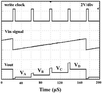
We can use another control method to avoid burning down the MOS or HBT device from the operation of the MVL circuit. We should require an extra write circuit MN0-MOS with a clock control gate and a saw-tooth wave at its input terminal, as those shown in Fig. 4 . The voltage to be stored is provided by the Vin signal and loaded to the main circuit by enabling the write clock in order. We use a square wave as the write clock that can turn on and off the MN0 alternately. During the bandwidth of the write clock, the corresponding voltage extracted from the saw-tooth wave is fed into this three-peak NDR circuit. Therefore, the output voltage across the three-peak NDR circuit is set to the nearest stable operating point according to this feed-in voltage. We can obtain different output voltage levels corresponding to different feed-in voltages by this way. Fig. 7 shows the waveforms of the write clock, Vin signal, and Vout result of this MVL circuit, which are extracted from the oscilloscope. We obtain four logic levels from VA to VD in order. The magnitudes of the four logic levels are the same as those shown in Fig. 6 . We also observe three transient states, which are the corresponding feed-in voltages. The other difficult problem is that we should preciously design the slope and magnitude of the saw-tooth input signal of this MVL circuit.
|
|
|
Fig. 7. Measured result of the MVL circuit using an extra write circuit along with a pulse control gate and a saw-tooth input signal. |
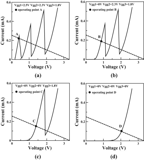
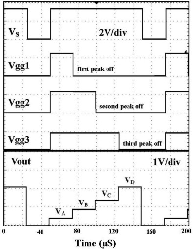
To overcome the transient-state effects, we propose another new control method in our NDR circuit. This concept is inspired from the forming method of three peaks in our novel BiCMOS-based NDR circuit that the peak can be controlled by the external voltage Vgg. Fig. 8 shows the four load-line analyses under three different Vgg conditions. Fig. 8(a) shows the initial condition and point A is the operating point. When we set Vgg1 at zero voltage and the other two voltages Vgg2 and Vgg3 remain unchanged, the operating point is located at point B, as shown in Fig. 8(b) . When we control both voltages Vgg1 and Vgg2 at zero voltage and keep the Vgg3 unchanged, the operating point is located at point C, as shown in Fig. 8(c) . Fig. 8(d) shows the case when all controlled voltages Vgg are turned off, the operating point is located at point D. This is resulted from the serial connection of the MN3 devices of three NDR circuits under the bias VS . It results in the fourth PDR segment still exists. Four conditions match perfectly the load line intersecting the three-peak I–V curve with operating points A, B, C, and D in order. Using this special peak-control method, we can obtain the four logic states shown as VA , VB , VC , and VD in order. In particular, there is no transient state when we transfer the logic state from one level to another.
|
|
|
Fig. 8. Load-line analysis of the peak-control method under four different Vgg conditions. |
Fig. 9 demonstrates the waveforms of the bias VS , control voltages Vgg, and Vout signal. Four logic states VA , VB , VC and VD are shown at the bottom of Fig. 9 . These logic levels are increased in step from VA to VD in sequence. Each logic corresponds to the relative Vgg condition. The magnitudes of the four logic levels are the same as those shown in Fig. 6 . The bias VS is inputted in a square wave, same as the control voltages Vgg. When one of the Vgg is set to zero voltage, the corresponding peak is turned off. Then the output level is transferred from one state to another. Therefore, we can control the logic state independently. If we want to transfer the logic level to the output one by one, we can design a read circuit by connecting a switch and a NMOS device with a clock control gate at the output terminal of this MVL circuit.
|
|
|
Fig. 9. Measured result of the MVL circuit using the peak-control method, showing four logic states without any transient levels. |
In particular, the output clearly gives four logic states without any transient levels existing between the logic levels. These logic values match well with the load-line analyses. If the zero voltage is added to this MVL circuit and regarded as “0” logic state, then we can define our MVL circuit as five logic states with {0, 1, 2, 3, 4}. The voltages from state “1” to “4” are corresponding to VA to VD , respectively.
4. Discussion
Because there is no transient state in our novel voltage-controlled MVL circuit, the power consumption is the smallest compared to the triggering-pulse control and saw-tooth input wave methods. The noise margin of each state is defined as the minimum value of the current difference between the operating point and the peak (or valley) position. For example, the current difference between point C and IV2 is 0.12 mA and the current difference between point C and IP3 is 0.37 mA, as shown in Fig. 6 . We should take the smaller one as the noise margin. Therefore, the noise margin for four logic levels VA , VB , VC and VD are estimated to be 0.04 mA, 0.17 mA, 0.12 mA, and 0.05 mA, respectively. The smallest noise margin occurs at VA level. Therefore, the noise margin of this circuit is 0.04 mA. However, this noise margin can be improved by inputting a higher Vgg1 value. If we set the Vgg1 value at 3 V, the IP1 value increases from 0.26 mA to 0.32 mA. Then the noise margin for state VA can be increased from 0.04 to 0.1 mA. On the other hand, we can design a constant current source as a load device to increase the noise margin. If we design a constant current source with 0.15 mA as the load, then the noise margin for four logic levels are estimated to be 0.11 mA, 0.23 mA, 0.12 mA, and 0.1 mA, respectively. The noise margin for this new design is about 0.1 mA.
Because this MVL circuit was fabricated using the standard 0.35 µm SiGe BiCMOS process, the aspect ratios (W/L) of the MOS device is a little higher. These parameters can be decreased by using a further scaled-down CMOS or BiCMOS process. For example, if we implement the circuit using 0.18 µm CMOS process, we redesign the parameters as WMN1 = 8 µm, WMN2 = 4 µm, WMN3 = 2 µm, LMN1,2,3 = 0.18 µm, and the HBT is replaced by a BJT device. The three peak currents are ranged between 0.2 mA and 0.5 mA by modulating the Vgg values. Its area can be reduced to 31.3 × 56.7 µm2 , which is about one third of the above implemented IC area. However, the operating frequency of this MOS-HBT-NDR cannot compare to the RTD device, which can be operated under several hundred gigahertz. However, if we design this MVL circuit using a more advanced process, the area of this MVL circuit can be decreased and the operating frequency can be improved.
5. Conclusions
We demonstrate a novel voltage-controlled MVL circuit, which is made of several Si MOS and SiGe HBT devices. Compared to the traditional RTD-based or RITD-based MVL circuit, our MVL circuit can be completely fabricated by the BiCMOS process without the need for an MBE system. We apply a special peak-control method to transfer the logic state. In particular, there are no transient states between the stable levels like those RTD-based MVL circuits shown in the reference. This new MVL circuit provides a possible solution to a complex system design using the mainstream ULSI technology. By considering the process integration, mass production, and reproduction of electrical characteristics of devices, our MVL design is easier and the fabrication cost is lower than the RTD-based circuit. To achieve higher speed and frequency, we can use a further advanced CMOS or BiCMOS process.
Acknowledgment
This work was financially supported by the National Science Council, Taiwan under contract no. NSC101-2221-E-415-026 . The authors would like to thank the Chip Implementation Center (CIC) of Taiwan for their great assistance in arranging the fabrication of this chip.
References
- [1] J. Lukasiewicz; On three valued-logic; L. Borkowski (Ed.), Selected Works, North-Holland, Amsterdam (1920), pp. 169–171
- [2] R.C.G. da Silva, H. Boudinov, L. Carro; A novel voltage-mode CMOS quaternary logic design; IEEE Trans. Electron Devices, 53 (6) (2006), pp. 1480–1483
- [3] N. Ramanan, V. Misra; Multivalued logic using a novel multichannel GaN MOS structure; IEEE Electron Dev. Lett, 32 (10) (2011), pp. 1379–1381
- [4] E. McCluskey; Logic design of multivalued I2L logic circuits; IEEE Trans. Comput, 28 (8) (1979), pp. 546–559
- [5] L.J. Micheel; Heterojunction bipolar technology for emitter-coupled multiple-valued logic in gigahertz adders and multipliers; Proceedings of IEEE Twenty-Second International Symposium on Multiple-Valued Logic (1992), pp. 18–26
- [6] M.E. Romero, E. Mazina Martins, R.R. dos Santos, M.E.D. Gonzalez; Universal set of CMOS gates for the synthesis of multiple valued logic digital circuits; IEEE Trans. Circuits Syst. I Regul. Pap, 61 (3) (2014), pp. 736–749
- [7] Y. Yasuda, Y. Tokuda, S. Zaima, K. Pak, T. Nakamura, A. Yoshida; Realization of quaternary logic circuits by n-channel MOS devices; IEEE J. Solid-State Circuits, 21 (1) (1986), pp. 162–168
- [8] P.K. Vasundara, K.S. Gurumurthy; Quaternary CMOS combinational logic circuits; International IEEE Conference on Information and Multimedia Technology (2009), pp. 538–542
- [9] A.K. Chowdhury, M. Razali, G.L.C. Wyai, L. Gopal, B. Madon, A.K. Singh; An analysis of MVL neural operators using feed forward backpropagation: realization and application of logic synthesis; International IEEE Conference on Smart Sensors and Application (2015), pp. 122–126
- [10] S. Shin, K.R. Kim; Multiple negative differential resistance devices with ultra-high peak-to-valley current ratio for practical multi-valued logic and memory applications; Jpn J. Appl. Phys, 54 (6S1) (2015), p. 06FG07
- [11] K.W. Current; Current-mode CMOS multiple-valued logic circuits; IEEE J. Solid-State Circuits, 29 (2) (1994), pp. 95–107
- [12] R. da Silva, H. Boudinov, L. Carro; A novel voltage-mode CMOS quaternary logic design; IEEE Trans. Electron Devices, 53 (6) (2006), pp. 1480–1483
- [13] M.H. Moaiyeri, R.F. Mirzaee, A. Doostaregan, K. Navi, O. Hashemipour; A universal method for designing low-power carbon nanotube FET-based multiple-valued logic circuits; IET Comput. Digit. Tech, 7 (4) (2013), pp. 167–181
- [14] J. Liang, L. Chen, J. Han, F. Lombardi; Design and evaluation of multiple valued logic gates using pseudo N-type carbon nanotube FETs; IEEE Trans. Nanotechnol, 13 (4) (2014), pp. 695–708
- [15] E. Dubrova; Multiple-valued logic in VLSI: challenges and opportunities; Proceedings of NORCHIP (99) (1999), pp. 340–350
- [16] P. Mazumder, S. Kulkarni, M. Bhattacharya, J.P. Sun, G. Haddad; Digital circuit applications of resonant tunneling devices; Proc. IEEE, 86 (4) (1998), pp. 664–686
- [17] H. Pettenghi, M.J. Avedillo, J.M. Quintana; Improved nanopipelined RTD adder using generalized threshold gates; IEEE Trans. Nanotechnol, 10 (1) (2011), pp. 155–162
- [18] P. Glösekötter, C. Pacha, K.F. Goser, W. Prost, S.O. Kim, H. van Husen, et al.; Circuit and application aspects of tunnelling devices in a MOBILE configuration; Int. J. Circuit Theory Appl, 20 (2003), pp. 453–468
- [19] A.C. Seabaugh, Y.C. Kao, H.T. Yuan; Nine-state resonant tunneling diode memory; IEEE Electron Dev. Lett, 13 (9) (1992), pp. 479–481
- [20] Z.X. Yan, M.J. Deen; A new resonant-tunnel diode-based multivalued memory circuit using a MESFET depletion load; IEEE J. Solid-State Circuits, 27 (1992), pp. 1198–1202
- [21] N. Jin, S.Y. Chung, R.M. Heyns, P.R. Berger, R. Yu, P.E. Thompson, et al.; Tri-state logic using vertically integrated Si resonant interband tunneling diodes with double NDR; IEEE Electron Dev. Lett, 25 (2004), pp. 646–648
- [22] S. Karmakar; Ternary logic gates using quantum dot gate FETs (QDGFETs); Silicon, 6 (3) (2014), pp. 169–178
- [23] A. Ramesh, T.A. Growden, P.R. Berger, R. Loo, W.B. Vandervorst Douhard, M. Caymax; Boron delta-doping dependence on Si/SiGe resonant interband tunneling diodes grown by chemical vapor deposition; IEEE Trans. Electron Devices, 59 (3) (2012), pp. 602–609
- [24] S.Y. Chung, N. Jin, R.E. Pavlovicz, R. Yu, P.R. Berger, P.E. Thompson; Analysis of the voltage swing for logic and memory applications in Si/SiGe resonant interband tunnel diodes grown by molecular beam epitaxy; IEEE Trans. Nanotechnol, 6 (2) (2007), pp. 158–163
- [25] S. Sudirgo, R.P. Nandgaonkar, B. Curanovic, J. Hebding, K.D. Hirschman, S.S. Islam, et al.; Monolithically integrated Si/SiGe resonant interband and tunneling diodes/CMOS MOBILE latch with high voltage swing; Solid State Electron, 48 (10/11) (2004), pp. 1907–1910
- [26] S.Y. Chung, N. Jin, P.R. Berger, R. Yu, P.E. Thompson, R. Lake, et al.; 3-terminal Si-based negative differential resistance circuit element with adjustable peak-to-valley current ratios using a monolithic vertical integration; Appl. Phys. Lett, 84 (14) (2004), pp. 2688–2690
- [27] K.J. Gan; Investigation of the combined current-voltage characteristics of two similar Esaki-Diode-Like devices; Jpn J. Appl. Phys, 42 (10) (2003), pp. 6354–6358
- [28] P.K. Tripathy, R.K. Dash, C.R. Tripathy; A dynamic programming approach for layout optimization of interconnection networks; Eng. Sci. Technol, 18 (2015), pp. 374–384
- [29] Y. Wei, J. Shen; Novel universal threshold logic gate based on RTD and its application; Microelectronics J., 42 (6) (2011), pp. 851–854
Document information
Published on 10/04/17
Licence: Other
Share this document
Keywords
claim authorship
Are you one of the authors of this document?
